Philips Semiconductors
Product specification
High speed CAN transceiver
TJA1041A
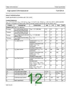
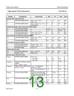
SYMBOL
Receiver data output (pin RXD)
IOH HIGH-level output current
PARAMETER
CONDITIONS
MIN.
TYP.
MAX.
UNIT
VRXD = VI/O − 0.4 V;
VI/O = VCC
−1
−3
−6
12
mA
mA
IOL
LOW-level output current
VRXD = 0.4 V; VTXD = VI/O
;
2
5
bus dominant
Standby and enable control inputs (pins STB and EN)
VIH
VIL
IIH
HIGH-level input voltage
LOW-level input voltage
HIGH-level input current
LOW-level input current
0.7VI/O
−
−
4
0
VCC + 0.3 V
−0.3
1
0.3VI/O
10
V
VSTB = VEN = 0.7VI/O
VSTB = VEN = 0 V
µA
µA
IIL
−
−1
Error and power-on indication output (pin ERR)
IOH
HIGH-level output current
VERR = VI/O − 0.4 V;
−4
−20
−50
µA
VI/O = VCC
IOL
LOW-level output current
VERR = 0.4 V
0.1
0.2
0.35
mA
Local wake-up input (pin WAKE)
IIH
IIL
HIGH-level input current
LOW-level input current
threshold voltage
VWAKE = VBAT − 1.9 V
VWAKE = VBAT − 3.1 V
VSTB = 0 V
−1
−5
−10
µA
µA
V
1
5
10
Vth
VBAT − 3 VBAT − 2.5 VBAT − 2
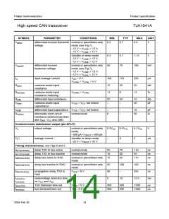
Inhibit output (pin INH)
∆VH
HIGH-level voltage drop
leakage current
IINH = −0.18 mA
0.05
0.2
0
0.8
5
V
IL
sleep mode
−
µA
Bus lines (pins CANH and CANL)
VO(dom)
dominant output voltage
VTXD = 0 V
pin CANH
pin CANL
3
3.6
1.4
−
4.25
V
V
V
0.5
−0.1
1.75
VO(dom)(m)
matching of dominant output
voltage
+0.15
(VCC − VCANH − VCANL
differential bus output voltage VTXD = 0 V (dominant);
(VCANH − VCANL 45 Ω < RL < 65 Ω
)
VO(dif)(bus)
1.5
−
3.0
+50
3
V
)
VTXD = VI/O (recessive); no −50
load
−
mV
V
VO(reces)
recessive output voltage
normal or pwon/listen-only
mode; VTXD = VI/O; no load
2
0.5VCC
0
standby or sleep mode; no −0.1
+0.1
V
load
IO(sc)
short-circuit output current
recessive output current
VTXD = 0 V (dominant)
pin CANH; VCANH = 0
pin CANL; VCANL = 40 V
−27 V < VCAN < 32 V
−40
40
−70
70
−
−95
95
mA
mA
mA
IO(reces)
−2.5
+2.5
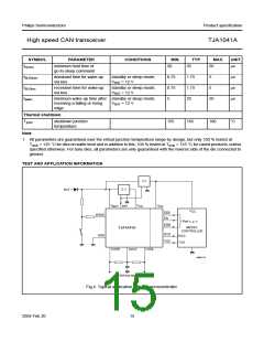
2004 Feb 20
13

 NXP [ NXP ]