Philips Semiconductors
Product specification
LIN transceiver
TJA1020
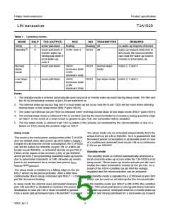
LIMITING VALUES
In accordance with the Absolute Maximum Rating System (IEC 60134); all voltages are referenced to pin GND.
SYMBOL
VBAT
TXD, VRXD, VNSLP DC voltage on pins TXD, RXD and NSLP
PARAMETER
CONDITIONS
MIN.
−0.3
MAX.
+40
UNIT
supply voltage on pin BAT
V
V
−0.3
−27
−1
+7
V
VLIN
DC voltage on pin LIN
+40
+40
−
V
VNWAKE
INWAKE
DC voltage on pin NWAKE
V
current on pin NWAKE (only relevant if
VNWAKE < VGND − 0.3 V; current will flow into
pin GND)
−15
mA
VINH
DC voltage on pin INH
−0.3
−50
VBAT + 0.3
+15
V
IINH
output current at pin INH
transient voltage on pin LIN (ISO7637)
virtual junction temperature
storage temperature
mA
V
Vtrt(LIN)
Tvj
−150
−40
+100
+150
°C
°C
Tstg
−55
+150
Vesd(HBM)
electrostatic discharge voltage; human body
model
note 1
note 2
on pins NWAKE, LIN and BAT
−4
+4
kV
kV
V
on pins RXD, NSLP, TXD and INH
−2
+2
Vesd(MM)
electrostatic discharge voltage; machine
model; all pins
−200
+200
Notes
1. Equivalent to discharging a 100 pF capacitor through a 1.5 kΩ resistor.
2. Equivalent to discharging a 200 pF capacitor through a 10 Ω resistor and a 0.75 µH coil. In the event of a discharge
from pin INH to pin BAT: −150 V < Vesd(MM) < +150 V.
THERMAL CHARACTERISTICS
According to IEC747-1.
SYMBOL
Rth(j-a)
PARAMETER
CONDITION
VALUE
UNIT
thermal resistance from junction to ambient in in free air
SO8 package
145
K/W
Rth(j-s)base
thermal resistance from junction to substrate in free air
bare die
tbf
K/W
QUALITY SPECIFICATION
Quality specification in accordance with “AEC - Q100”.
2002 Jul 17
9

 NXP [ NXP ]