Philips Semiconductors
Product specification
LIN transceiver
TJA1020
Setting pin NSLP HIGH during standby mode results in the
following events:
In the low slope mode the transmitter output stage drives
the LIN bus line with lengthened rise and fall slopes. This
will further reduce the already outstanding EME in the
normal slope mode. The low slope mode is perfectly suited
for applications where transmission speed is not critical.
The mode selection is done by the LIN transceiver after a
positive edge on pin NSLP, maintained for a certain time
period (tgotonorm). If pin TXD is LOW at that time, the low
slope mode is entered, otherwise the normal mode is
entered. The transition to the low slope mode will be
executed during an open pin TXD (fail-safe), a short-circuit
from pin TXD to ground (fail-safe) or an intended LOW
level of pin TXD programmed by the microcontroller. The
transmitter is enabled after a LOW-to-HIGH transition on
pin TXD. In the event of a short-circuit to ground on pin
TXD, the transmitter will be disabled.
• An immediate reset of the wake-up source flag; thus
releasing the possible strong pull-down at pin TXD
before the actual mode change (after tgotonorm) is
performed
• A change into normal slope mode if the HIGH level on
pin NSLP has been maintained for a certain time period
(tgotonorm) and pin TXD is HIGH
• A change into low slope mode if the HIGH level on pin
NSLP has been maintained for a certain time period
(tgotonorm) and pin TXD is pulled LOW by the application.
In the event of a short-circuit to ground or an open-wire
on pin TXD, the LIN output remains recessive (fail safe).
• A reset of the wake-up request signal on pin RXD if the
HIGH level on pin NSLP has been maintained for a
certain time period (tgotonorm).
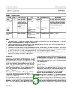
Wake-up
There are three ways to wake-up a TJA1020 which is in
sleep mode:
Normal slope mode
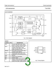
In the normal slope mode the transceiver is able to
transmit and receive data via the LIN bus line. The receiver
detects the data stream at the LIN bus input pin and
transfers it via pin RXD to the microcontroller (see Fig.1):
HIGH at a recessive level and LOW at a dominant level on
the bus. The receiver has a supply voltage related
threshold with hysteresis and an integrated filter to
suppress bus line noise. The transmit data stream of the
protocol controller at the TXD input is converted by the
transmitter into a bus signal with controlled slew rate and
wave shaping to minimize EME. The LIN bus output pin is
pulled HIGH via an internal slave termination resistor. For
a master application an external resistor in series with a
diode should be connected between pin INH or BAT on
one side and pin LIN on the other side.
1. Remote wake-up via a dominant bus state
2. Local wake-up via a negative edge at pin NWAKE
3. Mode change (pin NSLP is HIGH) from sleep mode to
normal slope/low slope mode.
Remote and local wake-up
A falling edge at pin NWAKE followed by a LOW level
maintained for a certain time period (tNWAKE) results in a
local wake-up. The pin NWAKE provides an internal
pull-up towards pin BAT.
If, during power-up, pin NWAKE is LOW for a certain
period of time (tNWAKE) this will also result in a local
wake-up.
A falling edge at pin LIN followed by a LOW level
maintained for a certain time period (tBUS) and a rising
edge at pin LIN respectively (see Fig.4) results in a remote
wake-up.
The normal slope mode is entered by a HIGH level on
pin TXD and a HIGH level on pin NSLP maintained for a
certain time period (tgotonorm), coming from the sleep or
standby mode.
After a local or remote wake-up pin INH is activated (it
goes HIGH) and the internal slave termination resistor is
switched on. The wake-up request is indicated by a LOW
active wake-up request signal on pin RXD to interrupt the
microcontroller.
The TJA1020 switches to sleep mode in case of a LOW
level on pin NSLP, maintained during a certain time period
(tgotosleep).
Low slope mode
The only difference between the normal slope mode and
the low slope mode is the transmitter behaviour.
2002 Jul 17
6

 NXP [ NXP ]