Philips Semiconductors
Product specification
LIN transceiver
TJA1020
FEATURES
General
GENERAL DESCRIPTION
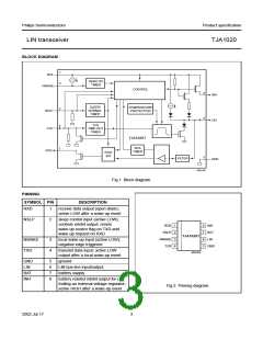
The TJA1020 is the interface between the LIN
master/slave protocol controller and the physical bus in a
Local Interconnect Network (LIN). It is primarily intended
for in-vehicle sub-networks using baud rates from 2.4 up to
20 Kbaud.
• Baud rate up to 20 Kbaud
• Very low ElectroMagnetic Emission (EME)
• High ElectroMagnetic Immunity (EMI)
• Low slope mode for an even further reduction of EME
• Passive behaviour in unpowered state
• Input levels compatible with 3.3 and 5 V devices
The transmit data stream of the protocol controller at the
TXD input is converted by the LIN transceiver into a bus
signal with controlled slew rate and wave shaping to
minimize EME. The LIN bus output pin is pulled HIGH via
an internal termination resistor. For a master application
an external resistor in series with a diode should be
connected between pin INH or pin BAT and pin LIN. The
receiver detects the data stream at the LIN bus input pin
and transfers it via pin RXD to the microcontroller.
• Integrated termination resistor for Local Interconnect
Network (LIN) slave applications
• Wake-up source recognition (local or remote).
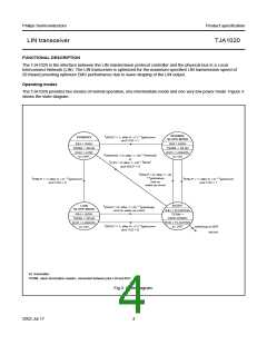
Low power management
In normal transceiver operation the TJA1020 can be
switched in the normal slope mode or the low slope mode.
In the low slope mode the TJA1020 lengthens the rise and
fall slopes of the LIN bus signal, thus further reducing the
already very low emission in normal slope mode.
• Very low current consumption in sleep mode with local
and remote wake-up.
Protections
• Transmit data (TXD) dominant time-out function
In sleep mode the power consumption of the TJA1020 is
very low, whereas in failure modes the power consumption
is reduced to a minimum.
• Bus terminal and battery pin protected against
transients in the automotive environment (ISO7637)
• Bus terminal short-circuit proof to battery and ground
• Thermally protected.
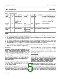
QUICK REFERENCE DATA
SYMBOL
VBAT
PARAMETER
MIN.
TYP. MAX. UNIT
supply voltage on pin BAT
5
12
3
27
8
V
IBAT
supply current on pin BAT in sleep mode
1
µA
supply current on pin BAT in standby mode; bus recessive
supply current on pin BAT in normal slope mode; bus recessive
supply current on pin BAT in normal slope mode; bus dominant
DC voltage on pin LIN
100
100
1
400
400
3.5
−
1000 µA
1000 µA
8.0
mA
V
VLIN
−27
−40
−4
+40
Tvj
virtual junction temperature
−
+150 °C
Vesd(HBM)
electrostatic discharge voltage; human body model;
pins NWAKE, LIN and BAT
−
+4
kV
ORDERING INFORMATION
TYPE
PACKAGES
NUMBER
NAME
DESCRIPTION
VERSION
SOT96-1
−
TJA1020T
TJA1020U
SO8
plastic small outline package; 8 leads; body width 3.9 mm
−
bare die; die dimensions 1480 × 1760 × 375 µm
2002 Jul 17
2

 NXP [ NXP ]