Philips Semiconductors
Product specification
New In Car Entertainment (NICE) car radio
TEA6845AH; TEA6845H
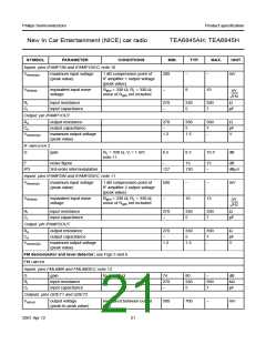
SYMBOL
PARAMETER
CONDITIONS
MIN.
TYP.
MAX.
UNIT
AGC peak detector output: pin T1FMAGC
Ich
charge current
−350
−600
−850
µA
Idis
discharge current
15
25
35
µA
PIN diode drive output: pin IFMAGC
Idrive drive current
Level voltage output: pin Vlevel
Vo = 0.5 to 4.0 V
8
11.5
950
15
mA
mV
Vth
threshold voltage for
narrow-band AGC
data byte 5: bit 7 = 1;
standard setting of level DAA
500
1400
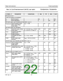
FM RF MIXER
Reference voltage: pin Vref(FMMIX)
Vref reference voltage
FM mode
AM mode
6.5
2.7
7.1
3.1
7.9
3.4
V
V
Inputs: pins FMMIXIN1 and FMMIXIN2; note 9
Vi(RF)(max)
maximum RF input
voltage
1 dB compression point of
FM mixer output voltage
(peak-to-peak value)
70
100
2.6
−
mV
Vi(n)(eq)
equivalent input noise
voltage
Rgen = 600 Ω; RL = 2.8 kΩ;
noise of Rgen not included
−
3.1
nV
-----------
Hz
Ri
Ci
input resistance
−
−
1.4
5
−
kΩ
input capacitance
7
pF
Outputs: pins MIX1OUT1 and MIX1OUT2; note 5
Ro
output resistance
output capacitance
mixer bias current
100
−
−
5
6
−
−
kΩ
pF
mA
V
Co
7
Ibias
FM mode
4.8
3
7.2
−
Vo(max)(p-p)
maximum output voltage
(peak-to-peak value)
FM mixer
gm(conv)
conversion
transconductance
8.5
12.5
18
mA
--------
V
gm(conv)(T)
conversion
−
−1 × 10⁻³
−
K−1
transconductance
variation with temperature
F
noise figure
−
3
4.6
−
dB
IP3
IRR
3rd-order intermodulation
image rejection ratio
116
25
119
30
dBµV
dB
−
IF AMPLIFIER 1
G
gain
RL = 330 Ω; Vi = 1 mV;
13.5
15.5
17.5
dB
note 10
F
noise figure
−
10
13
dB
IP3
3rd-order intermodulation
117
120
−
dBµV
2001 Apr 12
20

 NXP [ NXP ]