Philips Semiconductors
Product specification
New In Car Entertainment (NICE) car radio
TEA6845AH; TEA6845H
SYMBOL
PARAMETER
CONDITIONS
MIN.
TYP.
MAX.
UNIT
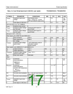
Inputs: pins IFAMP1IN and IFAMP1DEC; note 10
Vi(max)(p)
maximum input voltage
(peak value)
1 dB compression point of
IF amplifier 1 output voltage
(peak value)
200
−
−
mV
Vi(n)(eq)
equivalent input noise
voltage
Rgen = 330 Ω; RL = 330 Ω;
noise of Rgen not included
−
8
10
nV
-----------
Hz
Ri
Ci
input resistance
270
330
5
390
7
Ω
input capacitance
−
pF
Output: pin IFAMP1OUT
Ro
output resistance
270
−
330
5
390
7
Ω
Co
output capacitance
pF
V
Vo(max)(p)
maximum output voltage
(peak value)
1.2
1.5
−
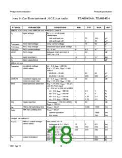
IF AMPLIFIER 2
G
gain
RL = 330 Ω; Vi = 1 mV;
6.5
8.5
10.5
dB
note 11
F
noise figure
−
13
15
dB
IP3
3rd-order intermodulation
127
130
−
dBµV
Inputs: pins IFAMP2IN and IFAMP2DEC; note 11
Vi(max)(p)
maximum input voltage
(peak value)
1 dB compression point of
IF amplifier 2 output voltage
(peak value)
500
−
−
mV
Vi(n)(eq)
equivalent input noise
voltage
Rgen = 330 Ω; RL = 330 Ω;
noise of Rgen not included
−
10
13
nV
-----------
Hz
Ri
Ci
input resistance
270
330
5
390
7
Ω
input capacitance
−
pF
Output: pin IFAMP2OUT
Ro
output resistance
270
−
330
5
390
7
Ω
Co
output capacitance
pF
V
Vo(max)(p)
maximum output voltage
(peak value)
1.2
1.5
−
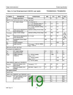
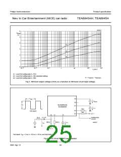
FM demodulator and level detector; see Figs 5 and 6
FM LIMITER
Inputs: pins FMLIMIN and FMLIMDEC; note 12
G
Ri
Ci
gain
Rgen = 50 Ω
74
270
−
80
330
5
−
dB
kΩ
pF
input resistance
input capacitance
390
7
Outputs: pins QDET1 and QDET2
Vo(p-p)
output voltage
(peak-to-peak value)
measured between output
pins
500
700
−
mV
2001 Apr 12
21

 NXP [ NXP ]