TDA8944J
2 x 7 W stereo BTL audio amplifier
Philips Semiconductors
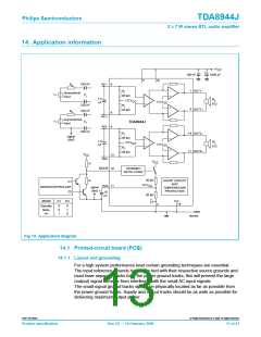
54 mm
idth
56 mm
OUT2−
ON
MUTE
OUT2+
+
−
10 µF
17
IN2−
IN2+
220 nF
1.5 nF
IN1−
IN1+
220 nF
V
CC
1
OUT1−
100 nF
1000 µF
GND
OUT1+
MGL951
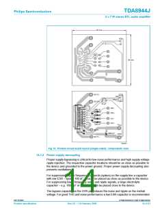
Fig 15. Printed-circuit board layout (single-sided); components view.
14.1.2 Power supply decoupling
Proper supply bypassing is critical for low-noise performance and high supply voltage
ripple rejection. The respective capacitor locations should be as close as possible to
the device and grounded to the power ground. Proper power supply decoupling also
prevents oscillations.
For suppressing higher frequency transients (spikes) on the supply line a capacitor
with low ESR – typical 100 nF – has to be placed as close as possible to the device.
For suppressing lower frequency noise and ripple signals, a large electrolytic
capacitor – e.g. 1000 µF or greater – must be placed close to the device.
The bypass capacitor on the SVR pin reduces the noise and ripple on the midrail
voltage. For good THD and noise performance a low ESR capacitor is recommended.
9397 750 06861
© Philips Electronics N.V. 2000. All rights reserved.
Product specification
Rev. 02 — 14 February 2000
14 of 21

 NXP [ NXP ]