TDA8944J
2 x 7 W stereo BTL audio amplifier
Philips Semiconductors
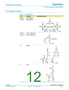
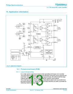
14. Application information
+V
CC
1000 µF
100 nF
3
16
220 nF
R
IN1−
8
s
−
+
1
4
OUT1−
R
i
Symmetrical
input
C
45 kΩ
i
−
+
1.5
nF
+
−
R
L
8 Ω
1/2 V
CC
1/2 V
CC
220 nF
220 nF
R
i
+
−
OUT1+
OUT2−
45 kΩ
R
s
6
9
IN1+
Asymmetrical
input
C
TDA8944J
i
IN2−
220 nF
−
+
14
R
i
signal
GND
45 kΩ
1/2 V
−
+
1.5
nF
+
−
R
L
8 Ω
CC
1/2 V
CC
R
i
+
−
17 OUT2+
45 kΩ
V
12
10
CC
IN2+
V
CC
R
MODE
STANDBY/
MUTE LOGIC
20 kΩ
R
SHORT CIRCUIT
AND
TEMPERATURE
PROTECTION
C1
1/2 V
SVR 11
CC
MICROCONTROLLER
C2
signal
GND
10
µF
20 kΩ
C1 C2
MODE
2
15
Standby
Mute
On
0
0
1
0
1
0
GND
MGL950
lupagwdeiht
Fig 14. Application diagram.
14.1 Printed-circuit board (PCB)
14.1.1 Layout and grounding
For a high system performance level certain grounding techniques are essential.
The input reference grounds have to be tied with their respective source grounds and
must have separate tracks from the power ground tracks; this will prevent the large
(output) signal currents from interfering with the small AC input signals.
The small-signal ground tracks should be physically located as far as possible from
the power ground tracks. Supply and output tracks should be as wide as possible for
delivering maximum output power.
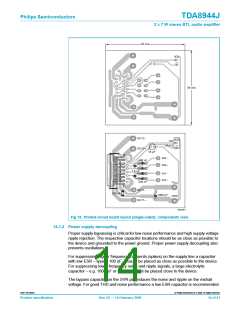
9397 750 06861
© Philips Electronics N.V. 2000. All rights reserved.
Product specification
Rev. 02 — 14 February 2000
13 of 21

 NXP [ NXP ]