TDA8920B
Philips Semiconductors
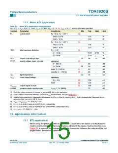
13.2 MODE pin
2 × 100 W class-D power amplifier
For pop-noise free start-up an RC time-constant must be applied on the MODE pin. The
bias-current setting of the VI-converter input is directly related to the voltage on the MODE
pin. In turn the bias-current setting of the VI converters is directly related to the DC output
offset voltage. Thus a slow dV/dt on the MODE pin results in a slow dV/dt for the DC
output offset voltage, resulting in pop-noise free start-up. A time-constant of 500 ms is
sufficient to guarantee pop-noise free start-up (see also Figure 4, 5 and 7).
13.3 Output power estimation
The achievable output powers in several applications (SE and BTL) can be estimated
using the following expressions:
SE:
2
R
L
× V × (1 – t
× f
)
osc
--------------------
P
min
R + 0.4
L
P
=
(1)
(2)
-----------------------------------------------------------------------------------------
2 × R
o(1%)
L
Maximum current (internally limited to 8 A):
V × (1 – t
× f
)
osc
P
min
I
=
-----------------------------------------------------
o(peak)
R + 0.4
L
BTL:
2
R
L
× 2V × (1 – t
× f
)
osc
--------------------
P
min
R + 0.8
L
P
=
(3)
(4)
--------------------------------------------------------------------------------------------
2 × R
o(1%)
L
Maximum current (internally limited to 8 A):
2V × (1 – t
× f
)
osc
p
min
I
=
---------------------------------------------------------
R + 0.8
o(peak)
L
Variables:
RL = load impedance
fosc = oscillator frequency
tmin = minimum pulse width (typical 150 ns)
VP = single-sided supply voltage (so, if supply is ±30 V symmetrical, then VP = 30 V)
Po(1%) = output power just at clipping
Po(10%) = output power at THD = 10 %
Po(10%) = 1.24 × Po(1%)
.
13.4 External clock
When using an external clock the following accuracy of the duty cycle of the external clock
has to be taken into account: 47.5 % < δ < 52.5 %.
9397 750 13356
© Koninklijke Philips Electronics N.V. 2004. All rights reserved.
Preliminary data sheet
Rev. 01 — 1 October 2004
16 of 34

 NXP [ NXP ]