TDA8920B
Philips Semiconductors
2 × 100 W class-D power amplifier
Table 7:
Static characteristics …continued
VP = ±27 V; fosc = 317 kHz; Tamb = 25 °C; unless otherwise specified.
Symbol
Parameter
Conditions
Min
Typ
Max Unit
Temperature protection
Tprot
Thys
temperature protection activation
hysteresis on temperature protection
-
-
150
20
-
-
°C
°C
[1] The circuit is DC adjusted at VP = ±12.5 V to ±30 V.
[2] With respect to SGND (0 V).
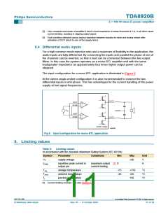
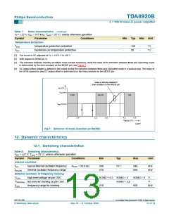
[3] The transition between Standby and Mute mode contain hysteresis, while the slope of the transition between Mute and Operating mode
is determined by the time-constant on the MODE pin; see Figure 7.
[4] DC output offset voltage is applied to the output during the transition between Mute and Operating mode in a gradual way. The slope of
the dV/dt caused by any DC output offset is determined by the time-constant on the MODE pin.
slope is directly related to
time-constant on the MODE pin
V
(V)
O
V
oo
(on)
STBY
MUTE
ON
V
(mute)
oo
0
0.8
2.2
3.0
4.2
5.5
V
MODE
(V)
coa021
Fig 7. Behavior of mode selection pin MODE.
12. Dynamic characteristics
12.1 Switching characteristics
Table 8:
Switching characteristics
VDD = ±27 V; Tamb = 25 °C; unless otherwise specified.
Symbol Parameter
Internal oscillator
Conditions
Min
Typ
Max
Unit
fosc
typical internal oscillator frequency
internal oscillator frequency range
ROSC = 30.0 kΩ
290
210
317
-
344
600
kHz
kHz
fosc(int)
External oscillator or frequency tracking
VOSC high-level voltage on pin OSC
VOSC(trip) trip level for tracking on pin OSC
SGND + 4.5 SGND + 5
SGND + 6
V
-
SGND + 2.5
-
V
ftrack
frequency range for tracking
210
-
600
kHz
9397 750 13356
© Koninklijke Philips Electronics N.V. 2004. All rights reserved.
Preliminary data sheet
Rev. 01 — 1 October 2004
13 of 34

 NXP [ NXP ]