Philips Semiconductors
Objective specification
Integrated PAL and PAL/NTSC TV
processors
TDA8360; TDA8361; TDA8362
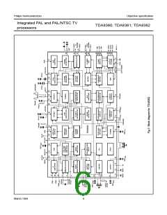
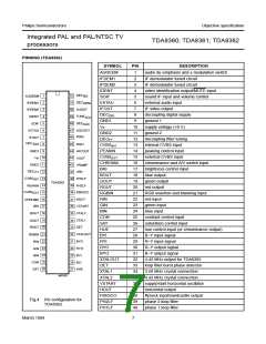
PINNING (TDA8362)
SYMBOL
PIN
DESCRIPTION
AUDEEM
IFDEM1
IFDEM2
IDENT
1
audio de-emphasis and ± modulation switch
IF demodulator tuned circuit
IF demodulator tuned circuit
video identification output/MUTE input
sound IF input and volume control
external audio input
2
3
4
DEC
DEC
1
2
52
51
50
49
AUDEEM
IFDEM1
IFDEM2
IDENT
BG
SOIF
5
EXTAU
IFOUT
DECDIG
GND1
VP
6
DEM
7
IF video output
AUOUT
TUNE
3
8
decoupling digital supply
ground 1
4
ADJ
9
5
48 DEC
AGC
SOIF
10
11
12
13
14
15
16
17
18
19
20
21
22
23
24
25
26
27
28
29
30
31
32
33
34
35
36
37
38
39
40
supply voltage (+8 V)
ground 2
EXTAU
6
47 AGCOUT
GND2
DECFT
CVBSINT
PEAKIN
CVBSEXT
CHROMA
BRI
IFIN2
IFIN1
46
45
7
IFOUT
decoupling filter tuning
internal CVBS input
DEC
DIG
8
GND1
9
44 AFCOUT
peaking control input
external CVBS input
chrominance and A/V switch input
brightness control input
blue output
V
P
10
43
42
VOUT
GND2 11
VRAMP
DEC
12
41 VFB
FT
BOUT
GOUT
ROUT
RGBIN
RIN
CVBS
40
39
13
14
15
16
PH1LF
PH2LF
INT
green output
TDA8362
PEAKIN
red output
CVBS
38 FBI/SCO
EXT
RGB insertion and blanking input
red input
HOUT
37
CHROMA
GIN
green input
BRI 17
36 VSTART
35 XTAL2
BIN
blue input
BOUT 18
CON
contrast control input
saturation control input
hue control input (or chrominance output)
B−Y input signal
19
20
XTAL1
34
GOUT
ROUT
SAT
33 DET
HUE
32 XTALOUT
31 BYO
RGBIN 21
BYI
22
RIN
RYI
R−Y input signal
RYO
R−Y output signal
23
24
30 RYO
29 RYI
28 BYI
27 HUE
GIN
BIN
BYO
B−Y output signal
XTALOUT
DET
4.43 MHz output for TDA8395
loop filter burst phase detector
3.58 MHz crystal connection
4.43 MHz crystal connection
supply/start horizontal oscillator
horizontal output
CON 25
26
SAT
XTAL1
XTAL2
VSTART
HOUT
FBI/SCO
PH2LF
PH1LF
MBC203
flyback input/sandcastle output
phase 2 loop filter
Fig.4 Pin configuration for
TDA8362.
phase 1 loop filter
March 1994
7

 NXP [ NXP ]