Philips Semiconductors
Product specification
CMOS single-chip 8-bit microcontrollers
80C31/80C51/87C51
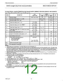
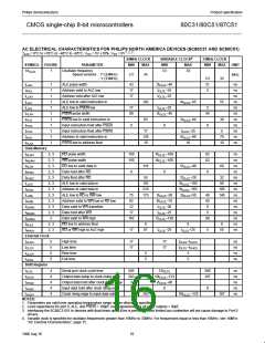
AC ELECTRICAL CHARACTERISTICS FOR PHILIPS NORTH AMERICA DEVICES (SC80C31 AND SC80C51)
1, 2, 3
T
amb
= 0°C to +70°C or –40°C to +85°C, V = 5V ±10%, V = 0V
CC SS
4
24MHz CLOCK
VARIABLE CLOCK
33MHz CLOCK
SYMBOL FIGURE
PARAMETER
MIN
MAX
MIN
MAX
MIN
MAX
UNIT
1/t
CLCL
1
Oscillator frequency
3.5
33
Speed versions : P (24MHz)
: Y (33MHz)
3.5
24
MHz
3.5
21
5
33
t
t
t
t
t
t
t
t
t
t
t
1
1
1
1
1
1
1
1
1
1
1
ALE pulse width
43
17
17
2t
–40
ns
ns
ns
ns
ns
ns
ns
ns
ns
ns
ns
LHLL
CLCL
Address valid to ALE low
Address hold after ALE low
ALE low to valid instruction in
ALE low to PSEN low
t
t
–25
AVLL
LLAX
LLIV
CLCL
CLCL
–25
102
65
4t
3t
–65
–60
55
30
CLCL
17
80
t
–25
5
LLPL
PLPH
PLIV
PXIX
PXIZ
AVIV
PLAZ
CLCL
PSEN pulse width
3t
CLCL
–45
45
PSEN low to valid instruction in
Input instruction hold after PSEN
Input instruction float after PSEN
Address to valid instruction in
PSEN low to address float
CLCL
0
0
0
17
128
10
t
–25
5
CLCL
5t
CLCL
–80
70
10
10
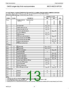
Data Memory
t
t
t
t
t
t
t
t
t
t
t
t
t
t
2, 3
2, 3
2, 3
2, 3
2, 3
2, 3
2, 3
2, 3
2, 3
2, 3
2, 3
3
RD pulse width
150
150
6t
–100
–100
82
82
ns
ns
ns
ns
ns
ns
ns
ns
ns
ns
ns
ns
ns
ns
RLRH
WLWH
RLDV
RHDX
RHDZ
LLDV
CLCL
WR pulse width
6t
CLCL
RD low to valid data in
Data hold after RD
118
5t
2t
–90
–28
60
CLCL
0
0
0
Data float after RD
55
32
90
CLCL
ALE low to valid data in
Address to valid data in
ALE low to RD or WR low
Address valid to WR low or RD low
Data valid to WR transition
Data hold after WR
183
210
175
8t
–150
–165
CLCL
CLCL
9t
105
140
AVDV
LLWL
75
92
3t
–50
–75
3t
CLCL
+50
40
45
0
CLCL
4t
AVWL
QVWX
WHQX
QVWH
RLAZ
WHLH
CLCL
12
t
–30
CLCL
CLCL
CLCL
17
t
–25
5
Data valid to WR high
RD low to address float
RD or WR high to ALE high
162
7t
–130
80
2, 3
2, 3
0
0
0
17
67
t
–25
t
+25
5
55
CLCL
CLCL
External Clock
t
t
t
t
5
5
5
5
High time
Low time
Rise time
Fall time
17
17
17
17
t
–t
ns
ns
ns
ns
CHCX
CLCX
CLCH
CHCL
CLCL CLCX
t
–t
CLCL CHCX
5
5
5
5
Shift Register
t
t
t
t
t
4
4
4
4
4
Serial port clock cycle time
505
283
3
12t
360
167
ns
ns
ns
ns
ns
XLXL
CLCL
Output data setup to clock rising edge
Output data hold after clock rising edge
Input data hold after clock rising edge
Clock rising edge to input data valid
10t –133
CLCL
QVXH
XHQX
XHDX
XHDV
2t
CLCL
–80
0
0
0
283
10t
–133
167
CLCL
NOTES:
1. Parameters are valid over operating temperature range unless otherwise specified.
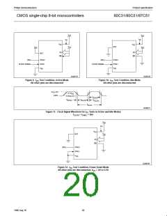
2. Load capacitance for port 0, ALE, and PSEN = 100pF, load capacitance for all other outputs = 80pF.
3. Interfacing the SC80C31/51 to devices with float times up to 45ns is permitted. This limited bus contention will not cause damage to Port 0
drivers.
4. Variable clock is specified for oscillator frequencies greater than 16MHz to 33MHz. For frequencies equal or less than 16MHz, see 16MHz
“AC Electrial Characteristics”, page 15.
16
1996 Aug 16

 NXP [ NXP ]