Philips Semiconductors
Product specification
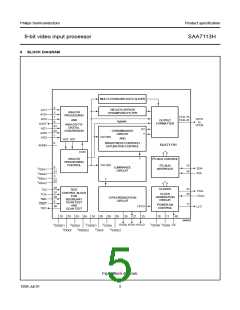
9-bit video input processor
SAA7113H
SYMBOL
PIN
I/O/P
DESCRIPTION
XTALI
32
I
input terminal for crystal oscillator or connection of external oscillator with CMOS
compatible square wave clock signal
VDDDA
VDDDE2
VSSDE2
TDO
TCK
33
34
35
36
37
38
39
40
P
P
P
O
I
digital positive supply voltage for internal crystal oscillator (+3.3 V)
digital supply voltage E2 (external pad supply 2; +3.3 V)
ground 2 for digital supply voltage input E (external pad supply)
test data output for boundary scan test; note 3
test clock for boundary scan test; note 3
TDI
I
test data input for boundary scan test; note 3
TMS
CE
I
test mode select input for boundary scan test or scan test; note 3
I
chip enable, ‘sleep mode’ with low power consumption if connected to ground
(internal pull-up); internal reset sequence is generated when released
VSSA2
VDDA2
AI21
41
42
43
44
P
P
I
ground for analog supply voltage channel 2
positive supply voltage for analog channel 2 (+3.3 V)
analog input 21
AI2D
I
differential analog input for AI21 and AI22; has to be connected to ground via a
capacitor; see application diagram of Fig.31
Notes
1. For board design without boundary scan implementation connect the TRST pin to ground.
2. This pin provides easy initialization of BST circuit. TRST can be used to force the Test Access Port (TAP) controller
to the TEST_LOGIC_RESET state (normal operation) at once.
3. In accordance with the IEEE1149.1 standard the pads TDI, TMS and TRST are input pads with an internal pull-up
transistor and TDO is a 3-state output pad.
1999 Jul 01
7

 NXP [ NXP ]