Philips Semiconductors
Product specification
9-bit video input processor
SAA7113H
7
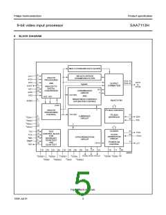
PINNING
SYMBOL
PIN
I/O/P
DESCRIPTION
AI22
1
2
3
4
5
I
P
P
I
analog input 22
VSSA1
VDDA1
AI11
ground for analog supply voltage channel 1
positive supply voltage for analog channel 1 (+3.3 V)
analog input 11
AI1D
I
differential analog input for AI11 and AI12; has to be connected to ground via a
capacitor; see application diagram of Fig.31
AGND
AI12
6
P
I
analog signal ground connection
7
analog input 12
TRST
AOUT
VDDA0
VSSA0
8
9
I
test reset input (active LOW), for boundary scan test; notes 1, 2 and 3
analog test output; for testing the analog input channels, 75 Ω termination possible
positive supply voltage (+3.3 V) for internal Clock Generation Circuit (CGC)
ground for internal clock generation circuit
O
P
P
O
10
11
VPO7 to
VPO4
12 to 15
digital VPO-bus output signal; higher bits of the 8-bit output bus. The output data
types of the VPO-bus are controlled via I2C-bus registers LCR2 to LCR24;
see Table 4. If I2C-bus bit VIPB = 1, the higher bits of the digitized input signal are
connected to these outputs, configured by the I2C-bus control signals
MODE3 to MODE0
VSSDE1
LLC
16
17
P
O
P
ground 1 or digital supply voltage input E (external pad supply)
line-locked system clock output (27 MHz)
VDDDE1
18
digital supply voltage E1 (external pad supply 1; +3.3 V)
VPO3 to
VPO0
19 to 22
O
digital VPO-bus output signal; lower bits of the 8-bit output bus. The output data types
of the VPO-bus are controlled via I2C-bus registers LCR2 to LCR24; see Table 4.
If I2C-bus bit VIPB = 1, the lower bits of the digitized input signal are connected to
these outputs, configured by the I2C-bus control signals MODE3 to MODE0
SDA
23
24
25
I/O
I
serial data input/output (I2C-bus) 5 V-compatible
serial clock input (I2C-bus) 5 V-compatible
SCL
RTCO
(I/)O real-time control output: contains information about actual system clock frequency,
field rate, odd/even sequence, decoder status, subcarrier frequency and phase and
PAL sequence (see external document “RTC Functional Description”, available on
request); the RTCO pin is enabled via I2C-bus bit OERT; this pin is also used as an
input pin for test purposes and has an internal pull-down resistor; do not
connect any pull-up resistor to this pin
RTS0
RTS1
26
27
(I/)O real-time signal output 0: multi functional output, controlled by I2C-bus bits
RTSE03 to RTSE00; see Table 49. RTS0 is strapped during power-on or CE driven
reset, defines which I2C-bus slave address is used; 0 = 48H for write, 49H for read,
external pull-down resistor of 3.3 kΩ is needed; 1 = 4AH for write, 4BH for read,
default slave address (default, internal pull-up)
I/O
real-time signal I/O terminal 1: multi functional output, controlled by I2C-bus bit
RTSE13 to RTSE10; see Table 50
VSSDI
VDDDI
VSSDA
XTAL
28
29
30
31
P
P
P
O
ground for internal digital core supply
internal core supply (+3.3 V)
digital ground for internal crystal oscillator
second terminal of crystal oscillator; not connected if external clock signal is used
1999 Jul 01
6

 NXP [ NXP ]