PDIUSBD12
USB interface device with parallel bus
Philips Semiconductors
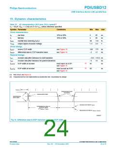
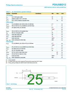
Table 17: AC characteristics (parallel interface)
Symbol Parameter
Conditions
Min
Max
Unit
ALE timings
tLH
ALE HIGH pulse width
20
10
−
−
ns
ns
ns
tAVLL
tLLAX
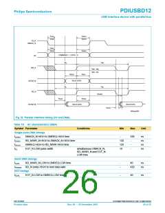
Write timings
address valid to ALE LOW time
−
ALE LOW to Address transition time
10
tCLWL
tWHCH
tAVWL
CS_N (DMACK_N) LOW to WR_N LOW time
0[1]
5
0[1]
130[2]
5
−
−
−
-
ns
ns
ns
ns
ns
ns
ns
ns
ns
ns
WR_N HIGH to CS_N (DMACK_N) HIGH time
A0 Valid to WR_N LOW time
tWHAX
tWL
WR_N HIGH to A0 transition time
WR_N LOW pulse width
write data setup time
write data hold time
−
−
−
−
−
-
20
tWDSU
tWDH
tWC
30
10
500[3]
write cycle time
t(WC - WD) write command to write data
600
Read timings
tCLRL
CS_N (DMACK_N) LOW to RD_N LOW time
0[1]
130[2]
5
−
ns
ns
ns
ns
ns
ns
ns
ns
ns
-
tRHCH
tAVRL
tRL
RD_N HIGH to CS_N (DMACK_N) HIGH time
A0 Valid to RD_N LOW time
RD_N LOW pulse width
−
0[1]
−
20
−
tRLDD
tRHDZ
tRC
RD_N LOW to Data Driven time
RD_N HIGH to Data Hi-Z time
read cycle time
−
20
20
−
−
500[3]
t(WC - RD) write command to read data
600
-
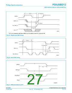
[1] Can be negative.
[2] For DMA access only on the module 64th byte and the second last (EOT-1)byte.
[3] The tWC and tRC timings are valid for back-to-back data access only.
Fig 17. ALE timing.
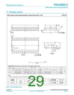
9397 750 09238
© Koninklijke Philips Electronics N.V. 2001. All rights reserved.
Product data
Rev. 08 — 20 December 2001
25 of 35

 NXP [ NXP ]