PDIUSBD12
USB interface device with parallel bus
Philips Semiconductors
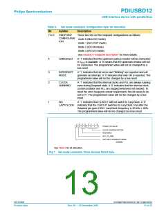
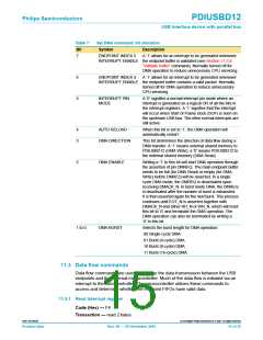
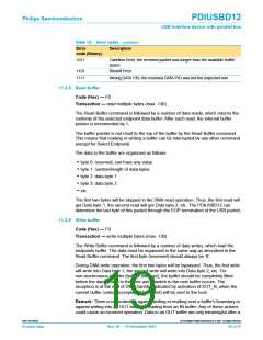
Table 7:
Set DMA command: bit allocation
Bit
Symbol
Description
7
ENDPOINT INDEX 5
A ‘1’ allows for an interrupt to be generated whenever
INTERRUPT ENABLE the endpoint buffer is validated (see Section 11.3.8
“Validate buffer” command). Normally turned off for
DMA operation to reduce unnecessary CPU servicing.
6
5
ENDPOINT INDEX 4
A ‘1’ allows for an interrupt to be generated whenever
INTERRUPT ENABLE the endpoint buffer contains a valid packet. Normally
turned off for DMA operation to reduce unnecessary
CPU servicing.
INTERRUPT PIN
MODE
A ‘0’ signifies a normal interrupt pin mode where an
interrupt is generated as a logical OR of all the bits in
the interrupt registers. A ‘1’ signifies that the interrupt
will occur when Start of Frame clock (SOF) is seen on
the upstream USB bus. The other normal interrupts are
still active.
4
3
AUTO RELOAD
When this bit is set to ‘1’, the DMA operation will
automatically restart.
DMA DIRECTION
This bit determines the direction of data flow during a
DMA transfer. A ‘1’ means external shared memory to
PDIUSBD12 (DMA Write); a ‘0’ means PDIUSBD12 to
the external shared memory (DMA Read).
2
DMA ENABLE
Writing a ‘1’ to this bit will start DMA operation through
the assertion of pin DMREQ. The main endpoint buffer
needs to be full (for DMA Read) or empty (for DMA
Write) before DMREQ will be asserted. In a single
cycle DMA mode, the DMREQ is deactivated upon
receiving DMACK_N. In burst mode DMA, the DMREQ
is deactivated after the number of burst is exhausted.
It is then asserted again for the next burst. This process
continues until EOT_N is asserted together with
DMACK_N and either RD_N or WR_N, which will reset
this bit to ‘0’ and terminate the DMA operation. The
DMA operation can also be terminated by writing a
‘0’ to this bit.
1 to 0
DMA BURST
Selects the burst length for DMA operation:
00 Single-cycle DMA
01 Burst (4-cycle) DMA
10 Burst (8-cycle) DMA
11 Burst (16-cycle) DMA
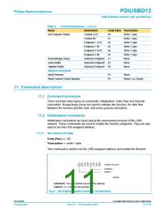
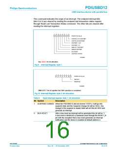
11.3 Data flow commands
Data flow commands are used to manage the data transmission between the USB
endpoints and the external microcontroller. Much of the data flow is initiated via an
interrupt to the microcontroller. The microcontroller utilizes these commands to
access and determine whether the endpoint FIFOs have valid data.
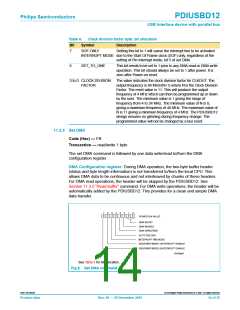
11.3.1 Read interrupt register
Code (Hex) — F4
Transaction — read 2 bytes
9397 750 09238
© Koninklijke Philips Electronics N.V. 2001. All rights reserved.
Product data
Rev. 08 — 20 December 2001
15 of 35

 NXP [ NXP ]