PDIUSBD12
USB interface device with parallel bus
Philips Semiconductors
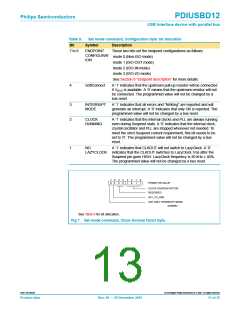
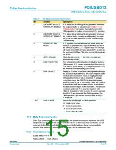
Table 6:
Clock division factor byte: bit allocation
Bit
Symbol
Description
7
SOF-ONLY
Setting this bit to 1 will cause the interrupt line to be activated
INTERRUPT MODE due to the Start Of Frame clock (SOF) only, regardless of the
setting of Pin-Interrupt mode, bit 5 of set DMA.
6
SET_TO_ONE
This bit needs to be set to 1 prior to any DMA read or DMA write
operation. This bit should always be set to 1 after power. It is
zero after Power-on reset.
3 to 0 CLOCK DIVISION
FACTOR
The value indicates the clock division factor for CLKOUT. The
output frequency is 48 MHz/(N+1) where N is the Clock Division
Factor. The reset value is 11. This will produce the output
frequency of 4 MHz which can then be programmed up or down
by the user. The minimum value is 1 giving the range of
frequency from 4 to 24 MHz. The minimum value of N is 0,
giving a maximum frequency of 48 MHz. The maximum value of
N is 11 giving a minimum frequency of 4 MHz. The PDIUSBD12
design ensures no glitching during frequency change. The
programmed value will not be changed by a bus reset.
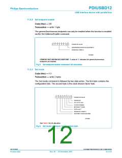
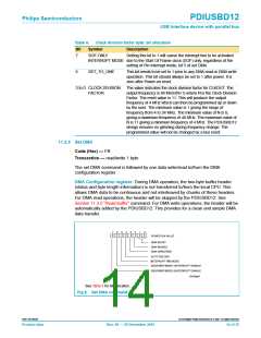
11.2.4 Set DMA
Code (Hex) — FB
Transaction — read/write 1 byte
The set DMA command is followed by one data write/read to/from the DMA
configuration register.
DMA Configuration register: During DMA operation, the two-byte buffer header
(status and byte length information) is not transferred to/from the local CPU. This
allows DMA data to be continuous and not interleaved by chunks of these headers.
For DMA read operations, the header will be skipped by the PDIUSBD12. See
Section 11.3.5 “Read buffer” command. For DMA write operations, the header will be
automatically added by the PDIUSBD12. This provides for a clean and simple DMA
data transfer.
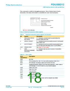
See Table 7 for bit allocation.
Fig 8. Set DMA command.
9397 750 09238
© Koninklijke Philips Electronics N.V. 2001. All rights reserved.
Product data
Rev. 08 — 20 December 2001
14 of 35

 NXP [ NXP ]