Philips Semiconductors
Product specification
Single-chip 8-bit microcontroller
80C552/83C552
Single-chip 8-bit microcontroller with 10-bit A/D, capture/compare timer, high-speed outputs, PWM
2
FEATURES
• 80C51 central processing unit
• I C-bus serial I/O port with byte oriented
master and slave functions
• Full-duplex UART compatible with the
standard 80C51
• 8k × 8 ROM expandable externally to 64k
bytes
• On-chip watchdog timer
• ROM code protection
• Three speed ranges:
– 3.5 to 16MHz
• An additional 16-bit timer/counter coupled
to four capture registers and three compare
registers
– 3.5 to 24MHz (ROM, ROMless only)
– 3.5 to 30MHz (ROM, ROMless only)
• Two standard 16-bit timer/counters
• 256 × 8 RAM, expandable externally to 64k
• Three operating ambient temperature
DESCRIPTION
bytes
ranges:
The 80C552/83C552 (hereafter generically
referred to as 8XC552) Single-Chip 8-Bit
Microcontroller is manufactured in an
advanced CMOS process and is a derivative
of the 80C51 microcontroller family. The
8XC552 has the same instruction set as the
80C51. Three versions of the derivative exist:
• Capable of producing eight synchronized,
timed outputs
– P83C552xBx: 0°C to +70°C
– P83C552xFx: –40°C to +85°C
(XTAL frequency max. 24 MHz)
• A 10-bit ADC with eight multiplexed analog
inputs
– P83C552xHx: –40°C to +125°C
(XTAL frequency max. 16 MHz)
• Two 8-bit resolution, pulse width
modulation outputs
• 83C552—8k bytes mask programmable
ROM
• Five 8-bit I/O ports plus one 8-bit input port
shared with analog inputs
• 80C552—ROMless version of the 83C552
• 87C552—8k bytes EPROM (described in a
separate chapter)
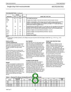
LOGIC SYMBOL
The 8XC552 contains a non-volatile 8k × 8
read-only program memory (83C552), a
volatile 256 × 8 read/write data memory, five
8-bit I/O ports, one 8-bit input port, two 16-bit
timer/event counters (identical to the timers of
the 80C51), an additional 16-bit timer coupled
to capture and compare latches, a 15-source,
two-priority-level, nested interrupt structure,
an 8-input ADC, a dual DAC pulse width
modulated interface, two serial interfaces
V
V
SS
DD
XTAL1
XTAL2
EA
ALE
PSEN
LOW ORDER
ADDRESS AND
DATA BUS
AV
AV
SS
DD
AVref+
AVref–
STADC
PWM0
PWM1
CT0I
CT1I
CT2I
CT3I
T2
RT2
SCL
SDA
2
(UART and I C-bus), a “watchdog” timer and
on-chip oscillator and timing circuits. For
systems that require extra capability, the
8XC552 can be expanded using standard
TTL compatible memories and logic.
ADC0-7
In addition, the 8XC552 has two software
selectable modes of power reduction—idle
mode and power-down mode. The idle mode
freezes the CPU while allowing the RAM,
timers, serial ports, and interrupt system to
continue functioning. The power-down mode
saves the RAM contents but freezes the
oscillator, causing all other chip functions to
be inoperative.
HIGH ORDER
ADDRESS AND
DATA BUS
CMSR0-5
RxD/DATA
TxD/CLOCK
INT0
INT1
T0
T1
WR
RD
CMT0
CMT1
RST
EW
The device also functions as an arithmetic
processor having facilities for both binary and
BCD arithmetic plus bit-handling capabilities.
The instruction set consists of over 100
instructions: 49 one-byte, 45 two-byte, and
17 three-byte. With a 16MHz (24MHz)
crystal, 58% of the instructions are executed
in 0.75µs (0.5µs) and 40% in 1.5µs (1µs).
Multiply and divide instructions require 3µs
(2µs).
2
1998 Aug 13

 NXP [ NXP ]