Philips Semiconductors
Product specification
Single-chip 8-bit microcontroller
80C552/83C552
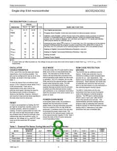
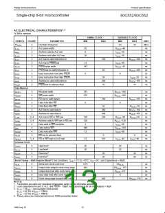
Serial Control Register (S1CON) – See Table 2
CR2 ENS1 STA
STO
SI
AA
CR1 CR0
S1CON (D8H)
Bits CR0, CR1 and CR2 determine the serial clock frequency that is generated in the master mode of operation.
Table 2. Serial Clock Rates
BIT FREQUENCY (kHz) AT f
OSC
2
2
CR2
CR1
CR0
6MHz
12MHz
16MHz
24MHz
30MHz
f
DIVIDED BY
OSC
0
0
0
0
1
1
1
1
0
0
1
1
0
0
1
1
0
1
0
1
0
1
0
1
23
27
31
37
6.25
50
47
54
63
62.5
71
83.3
100
17
94
117 1
256
1
1
1
1
107
125
150
25
200
400
134
156
188
224
192
160
960
120
60
1
1
75
12.5
100
200
31
250
500
1
1
1
1
133
267
1
1
100
0.24 < 62.5 0.49 < 62.5
0 < 255 0 < 254
0.65 < 55.6
0 < 253
0.98 < 50.0
0 <251
1.22 < 52.1
0 < 250
96 × (256 – (reload value Timer 1))
reload value Timer 1 in Mode 2.
NOTES:
2
2
1. These frequencies exceed the upper limit of 100kHz of the I C-bus specification and cannot be used in an I C-bus application.
2
2. At f
= 24MHz/ 30MHz the maximum I C bus rate of 100kHz cannot be realized due to the fixed divider rates.
OSC
1, 2, 3
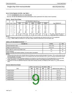
ABSOLUTE MAXIMUM RATINGS
PARAMETER
RATING
–65 to +150
–0.5 to +6.5
5.0
UNIT
°C
Storage temperature range
Voltage on any other pin to V
V
SS
Input, output DC current on any single I/O pin
mA
W
Power dissipation
1.0
(based on package heat transfer limitations, not device power consumption)
NOTES:
1. Stresses above those listed under Absolute Maximum Ratings may cause permanent damage to the device. This is a stress rating only and
functional operation of the device at these or any conditions other than those described in the AC and DC Electrical Characteristics section
of this specification is not implied.
2. This product includes circuitry specifically designed for the protection of its internal devices from the damaging effects of excessive static
charge. Nonetheless, it is suggested that conventional precautions be taken to avoid applying greater than the rated maxima.
3. Parameters are valid over operating temperature range unless otherwise specified. All voltages are with respect to V unless otherwise
SS
noted.
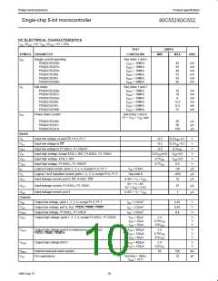
DEVICE SPECIFICATIONS
SUPPLY VOLTAGE (V)
FREQUENCY (MHz)
TYPE
MIN
4.5
4.5
4.5
4.5
4.5
4.5
MAX
5.5
5.5
5.5
5.5
5.5
5.5
MIN
3.5
3.5
3.5
3.5
3.5
3.5
MAX
16
TEMPERATURE RANGE (°C)
0 to +70
P83(0)C552EBx
P83(0)C552EFx
P83(0)C552EHx
P83(0)C552IBx
P83(0)C552IFx
P83(0)C552KBx
16
–40 to +85
16
–40 to +125
0 to +70
24
24
–40 to +85
30
0 to +70
9
1998 Aug 13

 NXP [ NXP ]