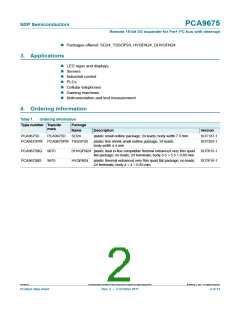
PCA9675
NXP Semiconductors
Remote 16-bit I/O expander for Fm+ I2C-bus with interrupt
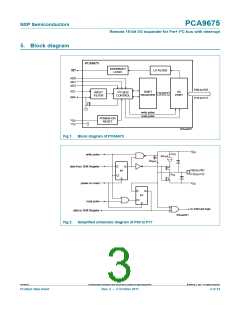
7. Functional description
Refer to Figure 1 “Block diagram of PCA9675”.
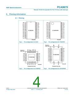
7.1 Device address
Following a START condition, the bus master must send the address of the slave it is
accessing and the operation it wants to perform (read or write). The address of the
PCA9675 is shown in Figure 7. Slave address pins AD2, AD1, and AD0 choose 1 of
64 slave addresses. To conserve power, no internal pull-up resistors are incorporated on
AD2, AD1, and AD0. Address values depending on AD2, AD1, and AD0 can be found in
Table 3 “PCA9675 address map”.
Remark: The General Call address (0000 0000b) and the Device ID address
(1111 100Xb) are reserved and cannot be used as device address. Failure to follow this
requirement will cause the PCA9675 not to acknowledge.
Remark: Reserved I2C-bus addresses must be used with caution since they can interfere
with:
• “reserved for future use” I2C-bus addresses (0000 011, 1111 101, 1111 110, 1111 111)
• slave devices that use the 10-bit addressing scheme (1111 0xx)
• High speed mode (Hs-mode) master code (0000 1xx)
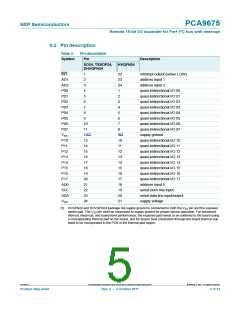
slave address
A6 A5 A4 A3 A2 A1 A0 R/W
programmable
002aab636
Fig 7. PCA9675 address
The last bit of the first byte defines the operation to be performed. When set to logic 1 a
read is selected, while a logic 0 selects a write operation.
When AD2, AD1 and AD0 are held to VDD or VSS, the same address as the PCF8575 is
applied.
7.1.1 Address maps
Table 3.
AD2
PCA9675 address map
AD1
SCL
SCL
SDA
SDA
SCL
SCL
SDA
SDA
AD0
VSS
VDD
VSS
VDD
VSS
VDD
VSS
VDD
A6
0
A5
0
A4
1
A3
0
A2
0
A1
0
A0
0
Address (hex)
VSS
VSS
VSS
VSS
VDD
VDD
VDD
VDD
20h
22h
24h
26h
28h
2Ah
2Ch
2Eh
0
0
1
0
0
0
1
0
0
1
0
0
1
0
0
0
1
0
0
1
1
0
0
1
0
1
0
0
0
0
1
0
1
0
1
0
0
1
0
1
1
0
0
0
1
0
1
1
1
PCA9675
All information provided in this document is subject to legal disclaimers.
© NXP B.V. 2011. All rights reserved.
Product data sheet
Rev. 2 — 3 October 2011
6 of 34

 NXP [ NXP ]