PCA9675
NXP Semiconductors
Remote 16-bit I/O expander for Fm+ I2C-bus with interrupt
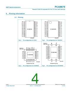
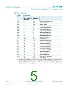
6.2 Pin description
Table 2.
Symbol
Pin description
Pin
Description
SO24, TSSOP24,
DHVQFN24
HVQFN24
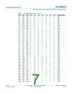
INT
1
22
23
24
1
interrupt output (active LOW)
address input 1
AD1
AD2
P00
P01
P02
P03
P04
P05
P06
P07
VSS
P10
P11
P12
P13
P14
P15
P16
P17
AD0
SCL
SDA
VDD
2
3
address input 2
4
quasi-bidirectional I/O 00
quasi-bidirectional I/O 01
quasi-bidirectional I/O 02
quasi-bidirectional I/O 03
quasi-bidirectional I/O 04
quasi-bidirectional I/O 05
quasi-bidirectional I/O 06
quasi-bidirectional I/O 07
supply ground
5
2
6
3
7
4
8
5
9
6
10
11
12[1]
13
14
15
16
17
18
19
20
21
22
23
24
7
8
9[1]
10
11
12
13
14
15
16
17
18
19
20
21
quasi-bidirectional I/O 10
quasi-bidirectional I/O 11
quasi-bidirectional I/O 12
quasi-bidirectional I/O 13
quasi-bidirectional I/O 14
quasi-bidirectional I/O 15
quasi-bidirectional I/O 16
quasi-bidirectional I/O 17
address input 0
serial clock line input
serial data line input/output
supply voltage
[1] HVQFN24 and DHVQFN24 package die supply ground is connected to both the VSS pin and the exposed
center pad. The VSS pin must be connected to supply ground for proper device operation. For enhanced
thermal, electrical, and board-level performance, the exposed pad needs to be soldered to the board using
a corresponding thermal pad on the board, and for proper heat conduction through the board thermal vias
need to be incorporated in the PCB in the thermal pad region.
PCA9675
All information provided in this document is subject to legal disclaimers.
© NXP B.V. 2011. All rights reserved.
Product data sheet
Rev. 2 — 3 October 2011
5 of 34

 NXP [ NXP ]