PCA9557
NXP Semiconductors
8-bit I2C-bus and SMBus I/O port with reset
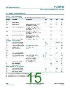
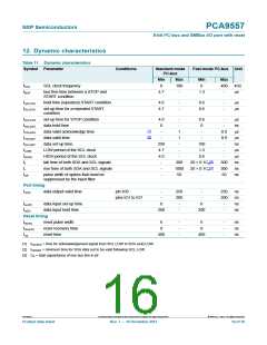
12. Dynamic characteristics
Table 11. Dynamic characteristics
Symbol Parameter
Conditions
Standard-mode
I2C-bus
Fast-mode I2C-bus Unit
Min
0
Max
100
-
Min
0
Max
400
-
fSCL
tBUF
SCL clock frequency
kHz
bus free time between a STOP and
START condition
4.7
1.3
s
tHD;STA
tSU;STA
hold time (repeated) START condition
4.0
4.7
-
-
0.6
0.6
-
-
s
s
set-up time for a repeated START
condition
tSU;STO
tHD;DAT
tVD;ACK
tVD;DAT
tSU;DAT
tLOW
tHIGH
tf
set-up time for STOP condition
data hold time
4.0
-
0.6
-
-
s
ns
s
s
ns
s
s
ns
ns
ns
0
-
0
[1]
[2]
data valid acknowledge time
data valid time
-
-
1
-
0.9
0.9
-
1
-
data set-up time
250
4.7
4.0
-
-
-
100
1.3
LOW period of the SCL clock
HIGH period of the SCL clock
fall time of both SDA and SCL signals
rise time of both SDA and SCL signals
-
-
0.6
-
[3]
[3]
300
1000
50
20 + 0.1Cb
20 + 0.1Cb
-
300
300
50
tr
-
tSP
pulse width of spikes that must be
suppressed by the input filter
-
Port timing
tv(Q)
data output valid time
pin IO0
-
-
250
-
-
250
ns
ns
ns
ns
pins IO1 to IO7
200
200
tsu(D)
th(D)
Reset timing
data input set-up time
0
-
-
0
-
-
data input hold time
200
200
tw(rst)
trec(rst)
trst
reset pulse width
6
0
-
-
-
6
0
-
-
-
ns
ns
ns
reset recovery time
reset time
400
400
[1] tVD;ACK = time for acknowledgement signal from SCL LOW to SDA (out) LOW.
[2] tVD;DAT = minimum time for SDA data out to be valid following SCL LOW.
[3] Cb = total capacitance of one bus line in pF.
PCA9557
All information provided in this document is subject to legal disclaimers.
© NXP B.V. 2013. All rights reserved.
Product data sheet
Rev. 7 — 10 December 2013
16 of 30

 NXP [ NXP ]