Philips Semiconductors
Preliminary specification
80C51 8-bit microcontroller
8K/256 OTP, 8 channel 10 bit A/D, I2C, PWM,
capture/compare, high I/O, low voltage (2.7V–5.5V), low power
P87C552
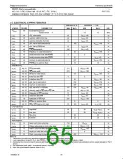
AC ELECTRICAL CHARACTERISTICS (Continued)
SYMBOL
PARAMETER
INPUT
OUTPUT
2
5
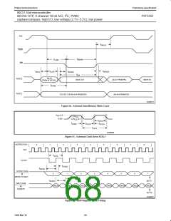
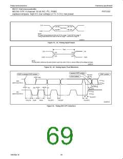
I C Interface (Refer to Figure 55)
1
t
t
t
t
t
t
t
t
t
t
t
t
t
t
START condition hold time
≥ 14 t
> 4.0µs
HD;STA
LOW
CLCL
CLCL
CLCL
1
SCL low time
≥ 16 t
≥ 14 t
> 4.7µs
1
SCL high time
> 4.0µs
HIGH
2
SCL rise time
≤ 1µs
–
RC
3
SCL fall time
≤ 0.3µs
≥ 250ns
≥ 250ns
≥ 250ns
≥ 0ns
< 0.3µs
FC
Data set-up time
> 20 t
– t
SU;DAT1
SU;DAT2
SU;DAT3
HD;DAT
SU;STA
SU;STO
BUF
CLCL
RD
FC
1
SDA set-up time (before rep. START cond.)
SDA set-up time (before STOP cond.)
Data hold time
> 1µs
> 8 t
CLCL
> 8 t
– t
CLCL
1
Repeated START set-up time
STOP condition set-up time
Bus free time
≥ 14 t
≥ 14 t
≥ 14 t
> 4.7µs
> 4.0µs
> 4.7µs
CLCL
CLCL
CLCL
1
1
2
SDA rise time
≤ 1µs
≤ 0.3µs
–
RD
3
SDA fall time
< 0.3µs
FD
NOTES:
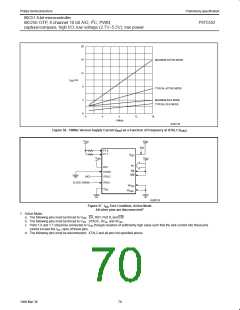
1. At 100 kbit/s. At other bit rates this value is inversely proportional to the bit-rate of 100 kbit/s.
2. Determined by the external bus-line capacitance and the external bus-line pull-resistor, this must be < 1µs.
3. Spikes on the SDA and SCL lines with a duration of less than 3 t
SCL = 400pF.
will be filtered out. Maximum capacitance on bus-lines SDA and
CLCL
4. t
= 1/f
= one oscillator clock period at pin XTAL1. For 62ns (42s) < t
< 285ns (16MHz > f
> 3.5MHz) the SI01 interface
CLCL
OSC
CLCL
OSC
2
meets the I C-bus specification for bit-rates up to 100 kbit/s.
5. These values are guaranteed but not 100% production tested.
66
1999 Mar 30

 NXP [ NXP ]