LPC2131/32/34/36/38
NXP Semiconductors
Single-chip 16/32-bit microcontrollers
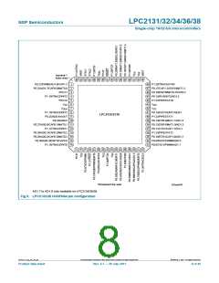
Table 3.
Pin description …continued
Symbol
Pin
Type
Description
P1.26/RTCK
24[6]
I/O
RTCK — Returned Test Clock output. Extra signal added to the JTAG port. Assists
debugger synchronization when processor frequency varies. Bidirectional pin with
internal pull-up. LOW on RTCK while RESET is LOW enables pins P1.31:26 to operate
as Debug port after reset.
P1.27/TDO
P1.28/TDI
P1.29/TCK
P1.30/TMS
P1.31/TRST
RESET
64[6]
60[6]
56[6]
52[6]
20[6]
57[7]
O
I
TDO — Test Data out for JTAG interface.
TDI — Test Data in for JTAG interface.
TCK — Test Clock for JTAG interface.
TMS — Test Mode Select for JTAG interface.
TRST — Test Reset for JTAG interface.
I
I
I
I
External reset input: A LOW on this pin resets the device, causing I/O ports and
peripherals to take on their default states, and processor execution to begin at address
0. TTL with hysteresis, 5 V tolerant.
XTAL1
XTAL2
RTCX1
RTCX2
VSS
62[8]
61[8]
3[9]
I
Input to the oscillator circuit and internal clock generator circuits.
Output from the oscillator amplifier.
O
I
Input to the RTC oscillator circuit.
5[9]
O
I
Output from the RTC oscillator circuit.
Ground: 0 V reference.
6, 18,
25, 42,
50
VSSA
VDD
59
I
I
I
Analog ground: 0 V reference. This should nominally be the same voltage as VSS, but
should be isolated to minimize noise and error.
23, 43,
51
3.3 V power supply: This is the power supply voltage for the core and I/O ports.
VDDA
7
Analog 3.3 V power supply: This should be nominally the same voltage as VDD but
should be isolated to minimize noise and error. This voltage is used to power the
on-chip PLL.
VREF
VBAT
63
49
I
I
ADC reference: This should be nominally the same voltage as VDD but should be
isolated to minimize noise and error. Level on this pin is used as a reference for A/D
and D/A convertor(s).
RTC power supply: 3.3 V on this pin supplies the power to the RTC.
[1] 5 V tolerant pad providing digital I/O functions with TTL levels and hysteresis and 10 ns slew rate control.
[2] 5 V tolerant pad providing digital I/O functions with TTL levels and hysteresis and 10 ns slew rate control. If configured for an input
function, this pad utilizes built-in glitch filter that blocks pulses shorter than 3 ns.
[3] Open drain 5 V tolerant digital I/O I2C-bus 400 kHz specification compatible pad. It requires external pull-up to provide an output
functionality.
[4] 5 V tolerant pad providing digital I/O (with TTL levels and hysteresis and 10 ns slew rate control) and analog input function. If configured
for an input function, this pad utilizes built-in glitch filter that blocks pulses shorter than 3 ns. When configured as an ADC input, digital
section of the pad is disabled.
[5] 5 V tolerant pad providing digital I/O (with TTL levels and hysteresis and 10 ns slew rate control) and analog output function. When
configured as the DAC output, digital section of the pad is disabled.
[6] 5 V tolerant pad with built-in pull-up resistor providing digital I/O functions with TTL levels and hysteresis and 10 ns slew rate control.
The pull-up resistor’s value ranges from 60 k to 300 k.
[7] 5 V tolerant pad providing digital input (with TTL levels and hysteresis) function only.
[8] Pad provides special analog functionality.
[9] When unused, the RTCX1 pin can be grounded or left floating. For lowest power leave it floating.
The other RTC pin, RTCX2, should be left floating.
LPC2131_32_34_36_38
All information provided in this document is subject to legal disclaimers.
© NXP B.V. 2011. All rights reserved.
Product data sheet
Rev. 5.1 — 29 July 2011
12 of 45

 NXP [ NXP ]