LPC2131/32/34/36/38
NXP Semiconductors
Single-chip 16/32-bit microcontrollers
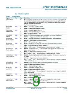
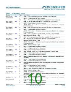
Table 3.
Symbol
Pin description …continued
Pin
Type
Description
P0.11/CTS1/
37[3]
I
CTS1 — Clear to Send input for UART1. Available in LPC2134/36/38.
CAP1.1/SCL1
I
CAP1.1 — Capture input for Timer 1, channel 1.
I/O
SCL1 — I2C1 clock input/output. Open drain output (for I2C-bus compliance)
DSR1 — Data Set Ready input for UART1. Available in LPC2134/36/38.
MAT1.0 — Match output for Timer 1, channel 0.
P0.12/DSR1/
38[4]
I
MAT1.0/AD1.3
O
I
AD1.3 — ADC 1, input 3. This analog input is always connected to its pin. Available in
LPC2134/36/38 only.
P0.13/DTR1/
MAT1.1/AD1.4
39[4]
O
O
I
DTR1 — Data Terminal Ready output for UART1. Available in LPC2134/36/38.
MAT1.1 — Match output for Timer 1, channel 1.
AD1.4 — ADC 1, input 4. This analog input is always connected to its pin. Available in
LPC2134/36/38 only.
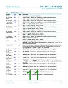
P0.14/DCD1/
EINT1/SDA1
41[3]
45[4]
I
DCD1 — Data Carrier Detect input for UART1. Available in LPC2134/36/38.
I
EINT1 — External interrupt 1 input.
I/O
SDA1 — I2C1 data input/output. Open drain output (for I2C-bus compliance).
RI1 — Ring Indicator input for UART1. Available in LPC2134/36/38.
EINT2 — External interrupt 2 input.
P0.15/RI1/
EINT2/AD1.5
I
I
I
AD1.5 — ADC 1, input 5. This analog input is always connected to its pin. Available in
LPC2134/36/38 only.
P0.16/EINT0/
46[2]
I
EINT0 — External interrupt 0 input.
MAT0.2/CAP0.2
O
I
MAT0.2 — Match output for Timer 0, channel 2.
CAP0.2 — Capture input for Timer 0, channel 2.
CAP1.2 — Capture input for Timer 1, channel 2.
SCK1 — Serial Clock for SSP. Clock output from master or input to slave.
MAT1.2 — Match output for Timer 1, channel 2.
CAP1.3 — Capture input for Timer 1, channel 3.
P0.17/CAP1.2/ 47[1]
SCK1/MAT1.2
I
I/O
O
I
P0.18/CAP1.3/ 53[1]
MISO1/MAT1.3
I/O
MISO1 — Master In Slave Out for SSP. Data input to SPI master or data output from
SSP slave.
O
MAT1.3 — Match output for Timer 1, channel 3.
MAT1.2 — Match output for Timer 1, channel 2.
P0.19/MAT1.2/ 54[1]
MOSI1/CAP1.2
O
I/O
MOSI1 — Master Out Slave In for SSP. Data output from SSP master or data input to
SSP slave.
I
CAP1.2 — Capture input for Timer 1, channel 2.
MAT1.3 — Match output for Timer 1, channel 3.
SSEL1 — Slave Select for SSP. Selects the SSP interface as a slave.
EINT3 — External interrupt 3 input.
P0.20/MAT1.3/ 55[2]
SSEL1/EINT3
O
I
I
P0.21/PWM5/
AD1.6/CAP1.3
1[4]
O
I
PWM5 — Pulse Width Modulator output 5.
AD1.6 — ADC 1, input 6. This analog input is always connected to its pin. Available in
LPC2134/36/38 only.
I
I
CAP1.3 — Capture input for Timer 1, channel 3.
P0.22/AD1.7/
2[4]
AD1.7 — ADC 1, input 7. This analog input is always connected to its pin. Available in
CAP0.0/MAT0.0
LPC2134/36/38 only.
I
CAP0.0 — Capture input for Timer 0, channel 0.
MAT0.0 — Match output for Timer 0, channel 0.
O
LPC2131_32_34_36_38
All information provided in this document is subject to legal disclaimers.
© NXP B.V. 2011. All rights reserved.
Product data sheet
Rev. 5.1 — 29 July 2011
10 of 45

 NXP [ NXP ]