LPC2131/32/34/36/38
NXP Semiconductors
Single-chip 16/32-bit microcontrollers
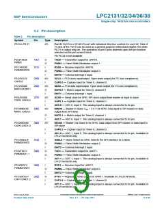
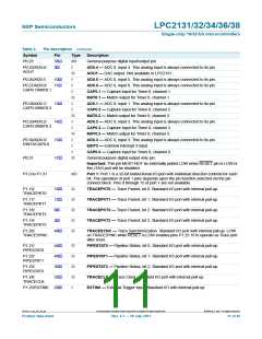
Table 3.
Symbol
P0.23
Pin description …continued
Pin
58[1]
9[5]
Type
Description
I/O
I
General purpose digital input/output pin.
P0.25/AD0.4/
AOUT
AD0.4 — ADC 0, input 4. This analog input is always connected to its pin.
AOUT — DAC output. Not available in LPC2131.
O
I
P0.26/AD0.5
10[4]
11[4]
AD0.5 — ADC 0, input 5. This analog input is always connected to its pin.
AD0.0 — ADC 0, input 0. This analog input is always connected to its pin.
CAP0.1 — Capture input for Timer 0, channel 1.
P0.27/AD0.0/
CAP0.1/MAT0.1
I
I
O
I
MAT0.1 — Match output for Timer 0, channel 1.
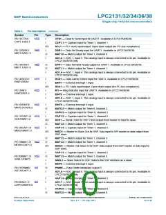
P0.28/AD0.1/
CAP0.2/MAT0.2
13[4]
14[4]
15[4]
17[6]
AD0.1 — ADC 0, input 1. This analog input is always connected to its pin.
CAP0.2 — Capture input for Timer 0, channel 2.
I
O
I
MAT0.2 — Match output for Timer 0, channel 2.
P0.29/AD0.2/
CAP0.3/MAT0.3
AD0.2 — ADC 0, input 2. This analog input is always connected to its pin.
CAP0.3 — Capture input for Timer 0, channel 3.
I
O
I
MAT0.3 — Match output for Timer 0, channel 3.
P0.30/AD0.3/
EINT3/CAP0.0
AD0.3 — ADC 0, input 3. This analog input is always connected to its pin.
EINT3 — External interrupt 3 input.
I
I
CAP0.0 — Capture input for Timer 0, channel 0.
P0.31
O
General purpose digital output only pin.
Important: This pin MUST NOT be externally pulled LOW when RESET pin is LOW or
the JTAG port will be disabled.
P1.0 to P1.31
I/O
Port 1: Port 1 is a 32-bit bidirectional I/O port with individual direction controls for each
bit. The operation of port 1 pins depends upon the pin function selected via the pin
connect block. Pins 0 through 15 of port 1 are not available.
P1.16/
TRACEPKT0
16[6]
12[6]
8[6]
O
O
O
O
O
TRACEPKT0 — Trace Packet, bit 0. Standard I/O port with internal pull-up.
TRACEPKT1 — Trace Packet, bit 1. Standard I/O port with internal pull-up.
TRACEPKT2 — Trace Packet, bit 2. Standard I/O port with internal pull-up.
TRACEPKT3 — Trace Packet, bit 3. Standard I/O port with internal pull-up.
P1.17/
TRACEPKT1
P1.18/
TRACEPKT2
P1.19/
TRACEPKT3
4[6]
P1.20/
TRACESYNC
48[6]
TRACESYNC — Trace Synchronization. Standard I/O port with internal pull-up. LOW
on TRACESYNC while RESET is LOW enables pins P1.25:16 to operate as Trace port
after reset.
P1.21/
PIPESTAT0
44[6]
40[6]
36[6]
32[6]
O
O
O
O
I
PIPESTAT0 — Pipeline Status, bit 0. Standard I/O port with internal pull-up.
PIPESTAT1 — Pipeline Status, bit 1. Standard I/O port with internal pull-up.
PIPESTAT2 — Pipeline Status, bit 2. Standard I/O port with internal pull-up.
TRACECLK — Trace Clock. Standard I/O port with internal pull-up.
EXTIN0 — External Trigger Input. Standard I/O with internal pull-up.
P1.22/
PIPESTAT1
P1.23/
PIPESTAT2
P1.24/
TRACECLK
P1.25/EXTIN0 28[6]
LPC2131_32_34_36_38
All information provided in this document is subject to legal disclaimers.
© NXP B.V. 2011. All rights reserved.
Product data sheet
Rev. 5.1 — 29 July 2011
11 of 45

 NXP [ NXP ]