Philips Semiconductors
Product specification
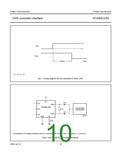
CAN controller interface
PCA82C250
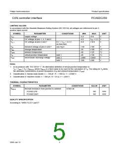
CHARACTERISTICS
VCC = 4.5 to 5.5 V; Tamb = −40 to +125 °C; RL = 60 Ω; I8 > −10 µA; unless otherwise specified; all voltages referenced
to ground (pin 2); positive input current; all parameters are guaranteed over the ambient temperature range by design,
but only 100% tested at +25 °C.
SYMBOL
PARAMETER
CONDITIONS
MIN.
TYP.
MAX.
UNIT
Supply
I3
supply current
dominant; V1 = 1 V
−
−
−
−
70
mA
recessive; V1 = 4 V;
R8 = 47 kΩ
14
mA
mA
µA
recessive; V1 = 4 V;
V8 = 1 V
−
−
−
18
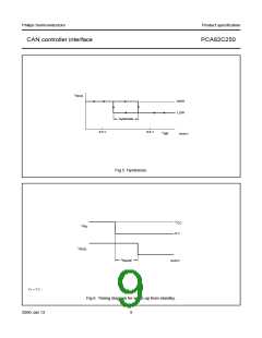
standby; Tamb < 90 °C;
100
170
note 1
DC bus transmitter
VIH
VIL
IIH
HIGH-level input voltage
LOW-level input voltage
HIGH-level input current
LOW-level input current
recessive bus voltage
output recessive
output dominant
V1 = 4 V
0.7VCC
−0.3
−200
−100
2.0
−
−
−
−
−
−
−
−
−
−
−
VCC + 0.3 V
0.3VCC
+30
−600
3.0
V
µA
µA
V
IIL
V1 = 1 V
V6,7
ILO
V1 = 4 V; no load
off-state output leakage current −2 V < (V6,V7) < 7 V
−5 V < (V6,V7) < 18 V
−2
+1
mA
mA
V
−5
+12
4.5
V7
CANH output voltage
CANL output voltage
V1 = 1 V
2.75
0.5
V6
V1 = 1 V
2.25
3.0
V
∆V6, 7
difference between output
voltage at pins 6 and 7
V1 = 1 V
1.5
V
V1 = 1 V; RL = 45 Ω;
1.5
−
V
VCC ≥ 4.9 V
V1 = 4 V; no load
V7 = −5 V; VCC ≤ 5 V
V7 = −5 V; VCC = 5.5 V
V6 = 18 V
−500
−
−
−
−
+50
mV
mA
mA
mA
Isc7
short-circuit CANH current
short-circuit CANL current
−
−
−
−105
−120
160
Isc6
DC bus receiver: V1 = 4 V; pins 6 and 7 externally driven; −2 V < (V6, V7) < 7 V; unless otherwise specified
Vdiff(r)
differential input voltage
(recessive)
−1.0
−1.0
−
−
+0.5
+0.4
V
V
−7 V < (V6, V7) < 12 V;
not standby mode
Vdiff(d)
differential input voltage
(dominant)
0.9
1.0
−
−
5.0
5.0
V
V
−7 V < (V6, V7) < 12 V;
not standby mode
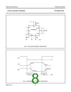
Vdiff(hys)
VOH
differential input hysteresis
see Fig.5
−
150
−
mV
V
HIGH-level output voltage
(pin 4)
I4 = −100 µA
0.8VCC
−
VCC
VOL
LOW-level output voltage (pin 4) I4 = 1 mA
I4 = 10 mA
0
0
5
−
−
−
0.2VCC
1.5
V
V
Ri
CANH, CANL input resistance
25
kΩ
2000 Jan 13
6

 NXP [ NXP ]