Philips Semiconductors
Product specification
CAN controller interface
PCA82C250
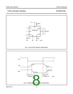
FUNCTIONAL DESCRIPTION
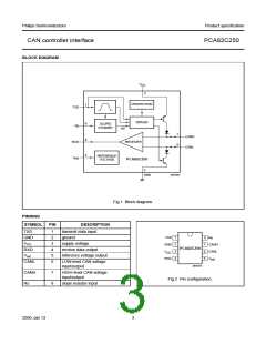
Pin 8 (Rs) allows three different modes of operation to be
selected: high-speed, slope control or standby.
The PCA82C250 is the interface between the CAN
protocol controller and the physical bus. It is primarily
intended for high-speed applications (up to 1 Mbaud) in
cars. The device provides differential transmit capability to
the bus and differential receive capability to the CAN
controller. It is fully compatible with the “ISO 11898”
standard.
For high-speed operation, the transmitter output
transistors are simply switched on and off as fast as
possible. In this mode, no measures are taken to limit the
rise and fall slope. Use of a shielded cable is
recommended to avoid RFI problems. The high-speed
mode is selected by connecting pin 8 to ground.
A current limiting circuit protects the transmitter output
stage against short-circuit to positive and negative battery
voltage. Although the power dissipation is increased
during this fault condition, this feature will prevent
destruction of the transmitter output stage.
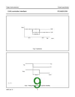
For lower speeds or shorter bus length, an unshielded
twisted pair or a parallel pair of wires can be used for the
bus. To reduce RFI, the rise and fall slope should be
limited. The rise and fall slope can be programmed with a
resistor connected from pin 8 to ground. The slope is
proportional to the current output at pin 8.
If the junction temperature exceeds a value of
approximately 160 °C, the limiting current of both
transmitter outputs is decreased. Because the transmitter
is responsible for the major part of the power dissipation,
this will result in a reduced power dissipation and hence a
lower chip temperature. All other parts of the IC will remain
in operation. The thermal protection is particularly needed
when a bus line is short-circuited.
If a HIGH level is applied to pin 8, the circuit enters a low
current standby mode. In this mode, the transmitter is
switched off and the receiver is switched to a low current.
If dominant bits are detected (differential bus voltage
>0.9 V), RXD will be switched to a LOW level.
The microcontroller should react to this condition by
switching the transceiver back to normal operation (via
pin 8). Because the receiver is slow in standby mode, the
first message will be lost.
The CANH and CANL lines are also protected against
electrical transients which may occur in an automotive
environment.
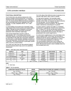
Table 1 Truth table of the CAN transceiver
SUPPLY
TXD
CANH
HIGH
CANL
LOW
BUS STATE
dominant
recessive
recessive
recessive
recessive
RXD
0
4.5 to 5.5 V
4.5 to 5.5 V
0
1 (or floating)
X(1)
floating
floating
floating
floating
floating
floating
1
<2 V (not powered)
2 V < VCC < 4.5 V
2 V < VCC < 4.5 V
X(1)
X(1)
X(1)
>0.75VCC
X(1)
floating if
floating if
VRs > 0.75VCC
VRs > 0.75VCC
Note
1. X = don’t care.
Table 2 Pin Rs summary
CONDITION FORCED AT PIN Rs
Rs > 0.75VCC
MODE
RESULTING VOLTAGE OR CURRENT AT PIN Rs
V
standby
IRs < 10 µA
0.4VCC < VRs < 0.6VCC
IRs < −500 µA
−10 µA < IRs < −200 µA
slope control
high-speed
VRs < 0.3VCC
2000 Jan 13
4

 NXP [ NXP ]