PI3VDP411LS
Digital Video Level Shifter from AC coupled
digital video input to a DVI/HDMI transmitter
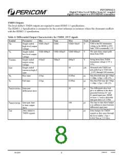
TMDS Outputs
The level shifter's TMDS outputs are required to meet HDMI 1.3 specifications.
The HDMI 1.3 Specification is assumed to be the correct reference in instances where this document conflicts
with the HDMI 1.3 specification.
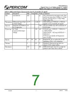
Table 6: Differential Output Characteristics for TMDS_OUT signals
Symbol
Parameter
Min
Nom
Max
Units Comments
VDD is the DC termination
voltage in the HDMI or DVI
Sink. VDD is nominally 3.3V
V
V
V
I
Single-ended
high level output
voltage
VDD-10mV
VDD
VDD+10mV
V
H
The open-drain output pulls
down from VDD.
Single-ended
low level output
voltage
VDD-600mV
450mV
VDD-500mV VDD-400mV
V
L
Swing down from TMDS
termination voltage (3.3V ±
10%)
Single-ended
output swing
voltage
500mV
600mV
50
V
SWING
Measured with TMDS out-
puts pulled up to VDD Max
_(3.6V) through 50Ω resistors.
Single-ended
current in high-Z
state
μA
OFF
Max Rise/Fall time @2.7Gbps
= 148ps. 125ps = 148-15%
T
T
Rise time
125ps
125ps
0.4Tbit
0.4Tbit
ps
ps
R
F
Max Rise/Fall time @2.7Gbps
= 148ps. 125ps = 148-15%
Fall time
This differential skew bud-
get is in addition to the skew
presented between D+ and
D- paired input pins. HDMI
revision 1.3 source allowable
intra-pair skew is 0.15Tbit.
T
Intra-pair
differential skew
30
ps
SKEW-INTRA
This lane-to-lane skew budget
is in addition to skew between
differential input pairs
T
T
Inter-pair lane-
to-lane output
skew
100
25
ps
ps
SKEW-INTER
JIT
Jitter added to
TMDS signals
Jitter budget for TMDS
signals as they pass through
the level shifter. 25ps =
0.056 Tbit at 2.25 Gb/s
PS8913D
11/05/08
08-0294
8

 PERICOM [ PERICOM SEMICONDUCTOR CORPORATION ]