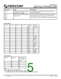
PI3VDP411LS
Digital Video Level Shifter from AC coupled
digital video input to a DVI/HDMI transmitter
Pin Name
Type
Description
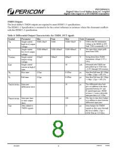
OUT_D2+
TMDS Differential output
HDMI 1.3 compliant TMDS output. OUT_D2+ makes
a differential output signal with OUT_D2–.
OUT_D2–
OUT_D1+
OUT_D1–
TMDS Differential output
TMDS Differential output
TMDS Differential output
HDMI 1.3 compliant TMDS output. OUT_D2– makes
a differential output signal with OUT_D2+.
HDMI 1.3 compliant TMDS output. OUT_D1+ makes
a differential output signal with OUT_D1–.
HDMI 1.3 compliant TMDS output. OUT_D1– makes
a differential output signal with OUT_D1+.
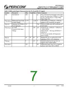
HPD_SINK
5V tolerance single-ended input Low Frequency, 0V to 5V (nominal) input signal. This
signal comes from the HDMI connector. Voltage High
indicates "plugged" state; voltage low indicated
"unplugged". HPD_SINK is pulled down by an
integrated 100K ohm put-down resistor.
HPD_SOURCE
SCL_SOURCE
3.3V single-ended output
HPD_SOURCE: 0V to 3.3V (nominal) output signal.
This is level-shifted version of the HPD_SINK signal.
Single-ended 3.3V open-drain
DDC I/O
3.3V DDC Data I/O. Pulled up by external termina-
tion to 3.3V. Connected to SCL_SINK through volt-
age-limiting integrated NMOS passgate.
SDA_SOURCE
SCL_SINK
SDA_SINK
DDC_EN
Single-ended 3.3V open-drain
DDC I/O
3.3V DDC Data I/O. Pulled up by external termination
to 3.3V. Connected to SDA_SINK through voltage-
limiting integrated NMOS passgate.
Single-ended 5V open-drain
DDC I/O
5V DDC Clock I/O. Pulled up by external termination
to 5V. Connected to SCL_SOURCE through voltage-
limiting integrated NMOS passgate.
Single-ended 5V open-drain
DDC I/O
5V DDC Data I/O. Pulled up by external termination
to 5V. Connected to SDA_SOURCE through voltage-
limiting integrated NMOS passgate.
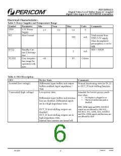
5.0V tolerant Single-ended input Enables bias voltage to the DDC passgate level shifter
gates. (May be implemented as a bias voltage connec-
tion to the DDC pass gates themselves.)
DDC_EN
0V
Passgate
Disabled
Enabled
3.3V
VDD
3.3V DC Supply
3.3V ± 10%
OC_2
(REXT)
3.3V single-ended control input Acceptable connections to OC_1 (REXT) pin are: Re-
sistor to GND; Resistor to 3.3V; NC. (Resistor should
be 0-ohm).
PS8913D
11/05/08
08-0294
4

 PERICOM [ PERICOM SEMICONDUCTOR CORPORATION ]