PI3VDP411LS
Digital Video Level Shifter from AC coupled
digital video input to a DVI/HDMI transmitter
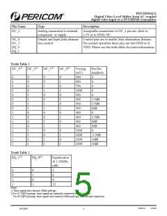
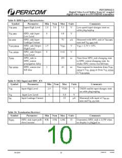
Electrical Characteristics
Table 3: Power Supplies and Temperature Range
Symbol
Parameter
Min
Nom
Max
Units
Comments
VDD
3.3V Power
Supply
3.0
3.3
3.6
V
ICC
Max Current
Total current from
VDD 3.3V supply
when de-emphasis/
pre-emphasis is set to
0dB.
100
mA
ICCQ
Standby Cur-
rent Consump-
tion
OE# = HIGH
2
mA
TCASE
Case tempera-
ture range for
operation with
spec.
-40
85
Celcius
Table 4: OE# Description
OE#
Device State
Comments
Asserted (low voltage)
Differential input buffers and output
buffers enabled. Input impedance =
50ꢀ
Normal functioning state for IN_D
to OUT_D level shifting function.
Unasserted (high voltage)
Low-power state.
Intended for lowest power condi-
tion when:
•
•
No display is plugged in or
The level shifted data path is
disabled
Differential input buffers and termina-
tion are disabled. Differential inputs
are in a high-impedance state.
HPD_SINK input and HPD_SOURCE
output are not affected by OE# SCL_
SOURCE, SCL_SINK, SDA_SOURCE
and SDA_SINK signals and functions are
not affected by OE#
OUT_D level-shifting outputs are
disabled.
OUT_D level-shifting outputs are in
high-impedence state.
Internal bias currents are turned off.
PS8913D
11/05/08
08-0294
6

 PERICOM [ PERICOM SEMICONDUCTOR CORPORATION ]