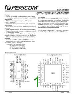
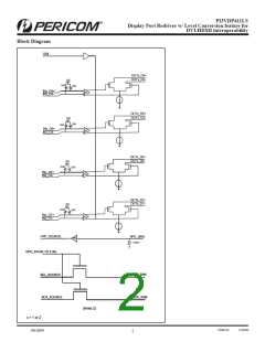
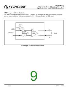
PI3VDP411LS
Digital Video Level Shifter from AC coupled
digital video input to a DVI/HDMI transmitter
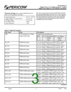
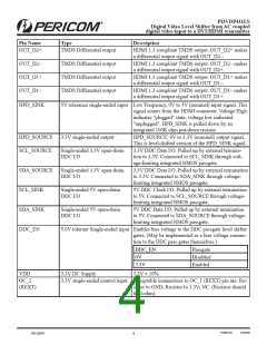
Pin Name
Type
Description
OC_3
Analog connection to external
component or supply
Acceptable connections to OC_3 pin are: short to
3.3V or to GND; NC.
OC_0
OC_1
EQ_0
EQ_1
Output and Input jitter elimina- Control pins are to enable Jitter elimination features.
tion control
For normal operation these pins are tied GND or to
VDD. Please see the truth tables for more information.
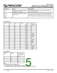
Truth Table 1
OC_3(2)
OC_2(1)
OC_1(1)
OC_0(1)
Vswing
Pre/De-
(mV)
emphasis
0
0
0
0
0
0
0
0
1
1
1
1
1
1
1
1
0
0
0
0
1
1
1
1
0
0
0
0
1
1
1
1
0
0
1
1
0
0
1
1
0
0
1
1
0
0
1
1
0
1
0
1
0
1
0
1
0
1
0
1
0
1
0
1
500
0
600
0
750
0
1000
500
0
0
500
1.5dB
3.5dB
6dB
0
500
500
400
400
3.5dB
6dB
9dB
0
400
400
1000
1000
1000
1000
-3.5dB
-6dB
-9dB
Truth Table 2
EQ_1(2)
EQ_0(1)
Equalization
@ 1.25GHz
(dB)
0
0
1
0
1
0
1
3
6
9
1
12
Notes:
1) These signals have internal 100kΩ pull-ups.
2) For 42-TQFN package, these signals are internally connected to GND directly.
For 48-TQFN package, these signals have internal 100kΩ pull-ups, with external connection.
PS8913D
11/05/08
08-0294
5

 PERICOM [ PERICOM SEMICONDUCTOR CORPORATION ]