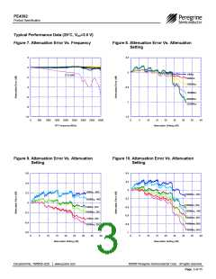
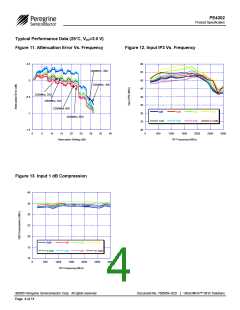
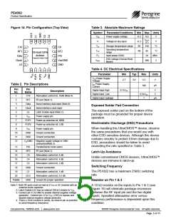
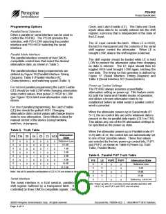
PE4302
Product Specification
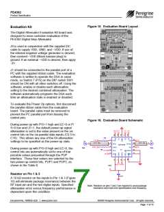
Figure 17. Serial Interface Timing Diagram
Table 7. 6-Bit Attenuator Serial Programming
Register Map
LE
Clock
B5
B4
B3
B2
B1
B0
C16
C8
C4
C2
C1
C0.5
Data
MSB
LSB
↑
↑
MSB (first in)
LSB (last in)
tLESUP
tLEPW
tSDSUP
tSDHLD
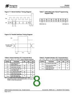
Figure 18. Parallel Interface Timing Diagram
LE
Parallel Data
C16:C0.5
tLEPW
tPDSUP
tPDHLD
Table 8. Serial Interface AC Characteristics
VDD = 3.0 V, -40° C < TA < 85° C, unless otherwise specified
Table 9. Parallel Interface AC Characteristics
VDD = 3.0 V, -40° C < TA < 85° C, unless otherwise specified
Symbol
Parameter
Min
Max
Unit
Symbol
tLEPW
Parameter
Min
10
Max
Unit
ns
Serial data clock fre-
quency (Note 1)
10
MHz
LE minimum pulse width
fClk
Data set-up time before
rising edge of LE
10
ns
Serial clock HIGH time
Serial clock LOW time
30
30
10
ns
ns
ns
tClkH
tClkL
tLESUP
tLEPW
tPDSUP
Data hold time after
falling edge of LE
10
ns
tPDHLD
LE set-up time after last
clock falling edge
LE minimum pulse width
30
10
ns
ns
Serial data set-up time
before clock rising edge
tSDSUP
Serial data hold time
after clock falling edge
10
ns
tSDHLD
Note: fClk is verified during the functional pattern test. Serial
programming sections of the functional pattern are clocked at
10 MHz to verify fclk specification.
©2005 Peregrine Semiconductor Corp. All rights reserved.
Document No. 70/0056~02D │ UltraCMOS™ RFIC Solutions
Page 8 of 11

 PSEMI [ Peregrine Semiconductor ]