PE4302
Product Specification
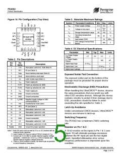
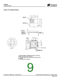
Figure 14. Pin Configuration (Top View)
Table 3. Absolute Maximum Ratings
Symbol
Parameter/Conditions
Min Max Units
VDD
Power supply voltage
-0.3
-0.3
-65
-40
4.0
V
VDD
+
VI
TST
TOP
PIN
Voltage on any input
V
0.3
Storage temperature range
150
85
°C
1
2
3
4
5
15
14
13
12
11
C16
RF1
C8
Operating temperature
range
°C
RF2
20-lead QFN
4x4mm
Input power (50ꢀ)
ESD voltage (Human Body
Model)
24
dBm
V
Data
Clock
LE
P/S
Exposed Solder Pad
Vss/GND
GND
VESD
500
Table 4. DC Electrical Specifications
Parameter
Min
Typ
Max
Units
V
VDD Power Supply
Voltage
2.7
3.0
3.3
IDD Power Supply
Current
Table 2. Pin Descriptions
100
µA
Pin
No.
Pin
Name
Digital Input High
Digital Input Low
Digital Input Leakage
0.7xVDD
V
V
Description
0.3xVDD
1
1
2
C16
RF1
Attenuation control bit, 16dB (Note 4).
RF port (Note 1).
µA
3
Data
Clock
LE
Serial interface data input (Note 4).
Serial interface clock input.
Latch Enable input (Note 2).
Power supply pin.
Exposed Solder Pad Connection
4
The exposed solder pad on the bottom of the
package must be grounded for proper device
operation.
5
6
VDD
7
PUP1
PUP2
VDD
Power-up selection bit, MSB.
Power-up selection bit, LSB.
Power supply pin.
Electrostatic Discharge (ESD) Precautions
8
When handling this UltraCMOS™ device, observe
the same precautions that you would use with
other ESD-sensitive devices. Although this device
contains circuitry to protect it from damage due to
ESD, precautions should be taken to avoid
exceeding the rate specified in Table 3.
9
10
11
12
GND
GND
Vss/GND
Ground connection.
Ground connection.
Negative supply voltage or GND
connection(Note 3)
13
14
P/S
RF2
C8
Parallel/Serial mode select.
RF port (Note 1).
Latch-Up Avoidance
15
Attenuation control bit, 8 dB.
Attenuation control bit, 4 dB.
Attenuation control bit, 2 dB.
Ground connection.
Unlike conventional CMOS devices, UltraCMOS™
devices are immune to latch-up.
16
C4
17
C2
Switching Frequency
18
GND
C1
The PE4302 has a maximum 25kHz switching
rate.
19
Attenuation control bit, 1 dB.
Attenuation control bit, 0.5 dB.
Ground for proper operation
20
C0.5
GND
Paddle
Resistor on Pin 1 & 3
Note 1: Both RF ports must be held at 0 VDC or DC blocked with an
external series capacitor.
A 10 kꢀ resistor on the inputs to Pin 1 & 3 (see
Figure 16) will eliminate package resonance
between the RF input pin and the two digital
inputs. Specified attenuation error versus
frequency performance is dependent upon this
condition.
2: Latch Enable (LE) has an internal 100 kꢀ resistor to VDD.
3: Connect pin 12 to GND to enable internal negative voltage
generator. Connect pin 12 to VSS (-VDD) to bypass and
disable internal negative voltage generator.
4. Place a 10 kꢀ resistor in series, as close to pin as possible
to avoid frequency resonance.
Document No. 70/0056~02D │ www.psemi.com
©2005 Peregrine Semiconductor Corp. All rights reserved.
Page 5 of 11

 PSEMI [ Peregrine Semiconductor ]