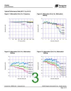
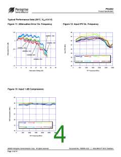
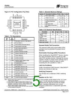
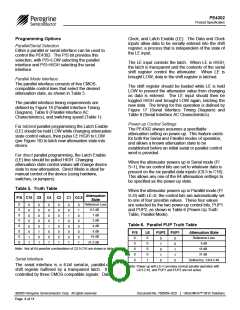
PE4302
Product Specification
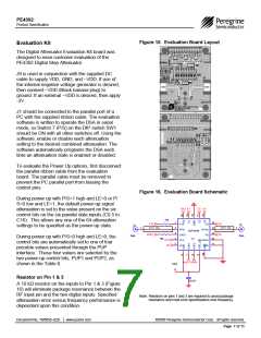
Figure 15. Evaluation Board Layout
Evaluation Kit
The Digital Attenuator Evaluation Kit board was
designed to ease customer evaluation of the
PE4302 Digital Step Attenuator.
J9 is used in conjunction with the supplied DC
cable to supply VDD, GND, and –VDD. If use of
the internal negative voltage generator is desired,
then connect –VDD (Black banana plug) to
ground. If an external –VDD is desired, then apply
-3V.
J1 should be connected to the parallel port of a
PC with the supplied ribbon cable. The evaluation
software is written to operate the DSA in serial
mode, so Switch 7 (P/S) on the DIP switch SW1
should be ON with all other switches off. Using the
software, enable or disable each attenuation
setting to the desired combined attenuation. The
software automatically programs the DSA each
time an attenuation state is enabled or disabled.
To evaluate the Power Up options, first disconnect
the parallel ribbon cable from the evaluation
board. The parallel cable must be removed to
prevent the PC parallel port from biasing the
control pins.
Figure 16. Evaluation Board Schematic
During power up with P/S=1 high and LE=0 or P/
S=0 low and LE=1, the default power-up signal
attenuation is set to the value present on the six
control bits on the six parallel data inputs (C0.5 to
C16). This allows any one of the 64 attenuation
settings to be specified as the power-up state.
C0.5 C1
C2 C4
10k
1
2
3
4
5
15
14
13
12
11
C16
Z=50 Ohm
C8
Z=50 Ohm
C16
C8
J5
J4
1
1
RFin
DATA
CLK
LE
RFout
PS
MLPQ4X4
U1
DATA
PS
SMA
SMA
During power up with P/S=0 high and LE=0, the
control bits are automatically set to one of four
possible values presented through the PUP
interface. These four values are selected by the
two power-up control bits, PUP1 and PUP2, as
shown in the Table 6.
10k
CLK
LE
Vss/GND
GND
PUP1 PUP2
VDD
Resistor on Pin 1 & 3
100 pF
A 10 kꢀ resistor on the inputs to Pin 1 & 3 (Figure
16) will eliminate package resonance between the
RF input pin and the two digital inputs. Specified
attenuation error versus frequency performance is
dependent upon this condition.
Note: Resistors on pins 1 and 3 are required to avoid package
resonance and meet error specifications over frequency.
Document No. 70/0056~02D │ www.psemi.com
©2005 Peregrine Semiconductor Corp. All rights reserved.
Page 7 of 11

 PSEMI [ Peregrine Semiconductor ]