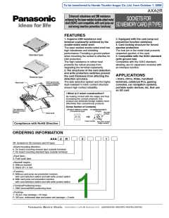
To be transferred to Honda Tsushin kogyo Co.,Ltd. from October 1, 2009
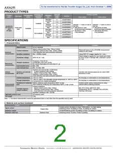
AXA2R
The CAD data of the products with a CAD Data mark can be downloaded from: http://panasonic-electric-works.net/ac
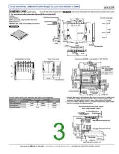
DIMENSIONS (Unit: mm)
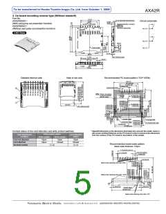
1. On board mounting standard type (Without standoff)
Part No.
AXA2R73061∗
*
1 0.08 (Standoff dimensions)
Circuit schematic
19.15
17.50
0.625
2.70
(With card jump-out prevention function)
AXA2R73021∗
(Without card jump-out prevention function)
9.375
2.50
0.60
(Signal/Detection contact)
0.10
No. 3
Terminal coplanarity
CAD Data
No. 2
No. 1
Card center
0.70
(14.65)
13.50
(3.40)
28.15
(17.50)
(2.10)
1.65 0.1
SD memory card
(Contact pitch) 2.50 0.1
(0.625)
14.55
27.95
Detailed internal view
View of set card
Recommended PC board pattern (TOP VIEW)
(30.15)
19.15 0.05
17.50 0.05
0.625 0.05
1.00 0.05
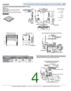
3
2.50 0.05 (Pitch)
: Pattern insulation
is recommended.
(Whole area)
(15.65)
7.48
: Pattern forbidden
area*2
2
1
10.37
1.60
8.58
(24.00)
12.25 0.05
12.45 0.05
1.75 0.05
1.55 0.05
SD memory card
1.60 0.05
0.60 0.05
0.40 0.05
Socket edge
PC board both side
0.60 0.05
0.40 0.05
1.60 0.05
Substrate edge
14.55 0.05
27.95 0.05
Through hole
*1 Standoff dimension is the dimension that takes into account the solder resist
or silk screen printing thickness on the PC board in order to preserve the
dimension from the surface of the PC board to the bottom of the socket.
*2 This is the pattern forbidden area. It is provided to prevent the signal contact
tips from contacting the substrate surface.
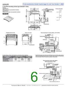
Contact status of the card detection and write protect switches
Write protect switch
Card attachment
condition
Card detection
switch
Write unable
Write enable
Open
Card not attached
Card attached
Open
Open
Open
Closed
1–3
Closed
Recommended metal mask pattern
Terminal number
1–2
Metal mask thickness: 120µm
17.5 0.05 (2.5×7)
2.5 0.05 (pitch)
1.65 0.05
9-1.0 0.03
6.27 0.05
5.88 0.05
1.31 0.03
1.55 0.03
1.75 0.03
Metal mask opening area ratio: 80%
Metal mask opening area ratio:100%
Socket edge
1.60 0.03
1.60 0.03
29.95 0.05
Metal mask opening area ratio: 75%
panasonic-electric-works.net/ac

 PANASONIC [ PANASONIC ]