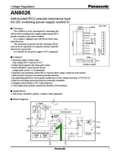
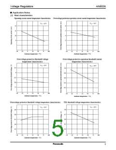
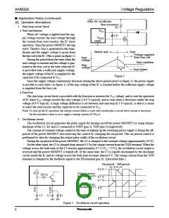
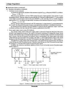
AN8026
Voltage Regulators
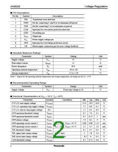
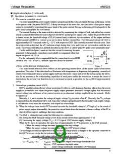
■ Pin Descriptions
Pin No.
Symbol
TDL
TOFF
TON
CLM
GND
VOUT
VCC
Description
Transformer reset detection
1
2
3
4
5
6
7
8
9
Pin for connecting C and R to set minimum off-period
Pin for connecting C to set minimum on-period
Input pin for overcurrent protection detection
Grounding pin
Output pin
Power supply voltage pin
OVP
FB
Input pin for overvoltage protection circuit
Photocoupler connection pin for error voltage feedback
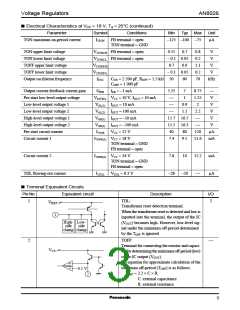
■ Absolute Maximum Ratings
Parameter
Symbol
VCC
Rating
35
Unit
V
Supply voltage
Peak output current
I6PEAK
PD
±1
A
Power dissipation
874
mW
°C
Operating ambient temperature *
Storage temperature *
Topr
−30 to +85
−55 to +150
Tstg
°C
Note) : Expect for the operating ambient temperature and storage temperature, all ratings are for T = 25°C.
*
a
■ Recommended Operating Range
Parameter
Supply voltage
Symbol
Range
Unit
VCC
From stop voltage to 34
V
■ Electrical Characteristics at VCC = 18 V, Ta = 25°C
Parameter
Symbol
Conditions
Min
Typ Max Unit
U.V.L.O. start supply voltage
V7START
13.4 14.9 16.4
V
V
U.V.L.O. operation stop supply voltage V7STOP
7.7
5.7
6.7
0.5
7.4
8.6
6.3
9.5
6.9
9.1
1
U.V.L.O. start-to-stop supply voltage
OVP operation threshold voltage
OVP operation threshold current
OVP release voltage
∆V7
V8OVP
I8OVP
V7OVP
V
7.9
V
0.75
8.2
mA
V
9
OVP operating circuit current 1
OVP operating circuit current 2
TDL threshold voltage
I7OVP1 VCC = 10 V, VOVP = 9.1 V
I7OVP2 VCC = 20 V, VOVP = 9.1 V
V1TDL
0.66 0.89 1.12
mA
mA
V
3.5
0.5
2
4.7
0.7
2.8
0
5.9
0.9
3.6
0.3
0.8
TDL upper limit clamp voltage
TDL lower limit clamp voltage
CLM threshold voltage
V1TDL/H ITDL = 3mA
V1TDL/L ITDL = −3mA
V4CLM
V
− 0.3
0.7
V
0.75
V
2

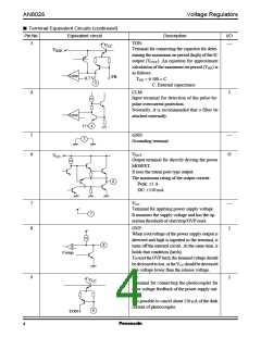
 PANASONIC [ PANASONIC ]