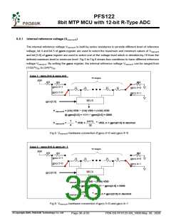
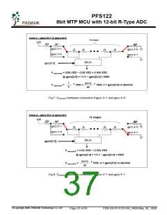
PFS122
8bit MTP MCU with 12-bit R-Type ADC
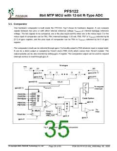
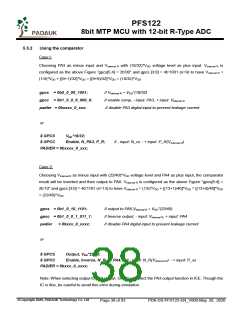
5.5. Comparator
One hardware comparator is built inside the PFS122; Fig.4 shows its hardware diagram. It can compare
signals between two pins or with either internal reference voltage Vinternal R or internal bandgap reference
voltage. The two signals to be compared, one is the plus input and the other one is the minus input. For the
minus input of comparator can be PA3, PA4, Internal bandgap 1.20 volt, PB6, PB7 or Vinternal R selected by bit
[3:1] of gpcc register, and the plus input of comparator can be PA4 or Vinternal R selected by bit 0 of gpcc
register.
The comparator result can be selected through gpcs.7 to forcibly output to PA0 whatever input or output state.
It can be a direct output or sampled by Timer2 clock (TM2_CLK) which comes from Timer2 module. The
output polarity can be also inverted by setting gpcc.4 register. The comparator output can be used to request
interrupt service or read through gpcc.6.
PA3/CIN-
PA4/CIN-
Bandgap
PB6/CIN-
PB7/CIN-
Fig.4: Hardware diagram of comparator
©Copyright 2020, PADAUK Technology Co. Ltd
Page 35 of 93
PDK-DS-PFS122-EN_V000-May 28, 2020

 PADAUK [ PADAUK Technology ]