UC3844, UC3845, UC2844, UC2845
MAXIMUM RATINGS
Rating
Symbol
Value
30
Unit
mA
A
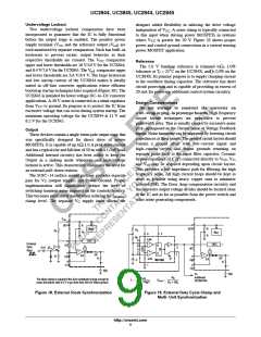
Total Power Supply and Zener Current
Output Current, Source or Sink (Note 1)
Output Energy (Capacitive Load per Cycle)
Current Sense and Voltage Feedback Inputs
Error Amp Output Sink Current
(I + I )
CC Z
I
O
1.0
W
5.0
− 0.3 to + 5.5
10
mJ
V
V
in
I
O
mA
Power Dissipation and Thermal Characteristics
D Suffix, Plastic Package, Case 751A
Maximum Power Dissipation @ T = 25°C
P
q
862
145
mW
A
D
JA
Thermal Resistance Junction−to−Air
R
°C/W
N Suffix, Plastic Package, Case 626
Maximum Power Dissipation @ T = 25°C
P
D
1.25
100
W
°C/W
A
Thermal Resistance Junction−to−Air
R
q
JA
Operating Junction Temperature
T
+ 150
°C
°C
J
Operating Ambient Temperature
UC3844, UC3845
T
A
0 to + 70
− 25 to + 85
UC2844, UC2845
Storage Temperature Range
T
stg
− 65 to + 150
°C
Stresses exceeding Maximum Ratings may damage the device. Maximum Ratings are stress ratings only. Functional operation above the
Recommended Operating Conditions is not implied. Extended exposure to stresses above the Recommended Operating Conditions may affect
device reliability.
1. Maximum Package power dissipation limits must be observed.
ELECTRICAL CHARACTERISTICS (V = 15 V, (Note 2), R = 10 k, C = 3.3 nF, T = T to T
(Note 3), unless otherwise noted.)
CC
T
T
A
low
high
UC284X
UC384X
Characteristics
REFERENCE SECTION
Reference Output Voltage (I = 1.0 mA, T = 25°C)
Symbol
Min
Typ
Max
Min
Typ
Max
Unit
V
ref
4.95
−
5.0
2.0
3.0
0.2
−
5.05
20
4.9
−
5.0
2.0
3.0
0.2
−
5.1
20
V
mV
mV
mV/°C
V
O
J
Line Regulation (V = 12 V to 25 V)
Reg
CC
line
load
S
Load Regulation (I = 1.0 mA to 20 mA)
Reg
−
25
−
25
O
Temperature Stability
T
−
−
−
−
Total Output Variation over Line, Load, Temperature
Output Noise Voltage (f = 10 Hz to kHz, T = 25°C)
V
ref
4.9
−
5.1
−
4.82
−
5.18
−
V
n
50
50
mV
J
Long Term Stability (T = 125°C for 1000 Hours)
S
−
5.0
− 85
−
−
5.0
− 85
−
mV
mA
A
Output Short Circuit Current
I
− 30
− 180
− 30
− 180
SC
OSCILLATOR SECTION
Frequency
f
kHz
osc
47
46
52
−
57
60
47
46
52
−
57
60
T = 25°C
J
T = T
to T
high
A
low
Frequency Change with Voltage (V = 12 V to 25 V)
Df
Df
D
D
−
−
0.2
5.0
1.0
−
−
0.2
5.0
1.0
%
%
CC
osc/
V
Frequency Change with Temperature
−
−
osc/
T
T = T
to T
A
low
high
Oscillator Voltage Swing (Peak−to−Peak)
Discharge Current (V = 2.0 V, T = 25°C)
V
−
−
1.6
−
−
−
−
1.6
−
−
V
osc
I
dischg
10.8
10.8
mA
osc
J
ERROR AMPLIFIER SECTION
Voltage Feedback Input (V = 2.5 V)
V
2.45
−
2.5
−0.1
90
2.55
−1.0
−
2.42
−
2.5
−0.1
90
2.58
−2.0
−
V
O
FB
Input Bias Current (V = 2.7 V)
I
IB
mA
dB
FB
Open Loop Voltage Gain (V = 2.0 V to 4.0 V)
A
VOL
65
65
O
2. Adjust V above the Startup threshold before setting to 15 V.
CC
3. Low duty cycle pulse techniques are used during test to maintain junction temperature as close to ambient as possible.
T
low
= 0°C for UC3844, UC3845
−25°C for UC2844, UC2845
T
high
= +70°C for UC3844, UC3845
+85°C for UC2844, UC2845
http://onsemi.com
2

 ONSEMI [ ONSEMI ]