NVHL020N120SC1
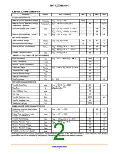
ELECTRICAL CHARACTERISTICS
Parameter
Symbol
Test Conditions
Min
Typ
Max
Unit
OFF CHARACTERISTICS
Drain−to−Source Breakdown Voltage
V
V
I
= 0 V, I = 1 mA
1200
−
−
−
V
(BR)DSS
GS
D
Drain−to−Source Breakdown Voltage
Temperature Coefficient
V
/T
= 1 mA, referenced to 25_C
−
900
mV/_C
(BR)DSS
J
D
Zero Gate Voltage Drain Current
I
−
−
−
−
−
−
100
250
1
ꢂ
A
V
GS
V
GS
V
GS
= 0 V, V = 1200 V, T = 25_C
DSS
DS
J
= 0 V, V = 1200 V, T = 175_C
DS
J
Gate−to−Source Leakage Current
ON CHARACTERISTICS
I
= +25/−15 V, V = 0 V
DS
ꢂ
A
GSS
Gate Threshold Voltage
V
R
V
= V , I = 20 mA
1.8
−5
−
2.7
−
4.3
+20
28
50
−
V
V
GS(th)
GS
DS
D
Recommended Gate Voltage
Drain−to−Source On Resistance
V
GOP
V
GS
V
GS
V
DS
= 20 V, I = 60 A, T = 25_C
20
35
28
mꢀ
DS(on)
D
J
= 20 V, I = 60 A, T = 175_C
−
D
J
Forward Transconductance
g
FS
= 10 V, I = 60 A
−
S
D
CHARGES, CAPACITANCES & GATE RESISTANCE
Input Capacitance
Output Capacitance
Reverse Transfer Capacitance
Total Gate Charge
C
V
= 0 V, f = 1 MHz, V = 800 V
−
−
−
−
−
−
−
−
2890
260
22
−
−
−
−
−
−
−
−
pF
nC
ISS
GS
GS
DS
C
OSS
RSS
C
Q
V
= −5/20 V, V = 600 V, I = 80 A
203
33
G(tot)
DS
D
Threshold Gate Charge
Gate−to−Source Charge
Gate−to−Drain Charge
Gate Resistance
Q
G(th)
Q
66
GS
GD
Q
47
R
f = 1 MHz
1.81
ꢀ
G
SWITCHING CHARACTERISTICS
Turn-On Delay Time
Rise Time
t
t
V
D
= −5/20 V, V = 800 V,
−
−
−
−
−
−
−
25
57
−
−
−
−
−
−
−
ns
d(on)
GS
DS
I
= 80 A, R = 2 ꢀ,
G
t
r
Inductive Load
Turn−Off Delay Time
Fall Time
45
d(off)
t
f
11
Turn-On Switching Loss
Turn-Off Switching Loss
Total Switching Loss
E
2718
326
3040
ꢂ
J
ON
OFF
TOT
E
E
DRAIN−SOURCE DIODE CHARACTERISTICS
Continuous Drain−to−Source Diode
I
V
V
= −5 V, T = 25_C
−
−
−
−
54
A
A
SD
GS
J
Forward Current
Pulsed Drain−to−Source Diode
Forward Current (Note 2)
I
= −5 V, T = 25_C
412
SDM
GS
J
Forward Diode Voltage
V
V
V
= −5 V, I = 30 A, T = 25_C
−
−
−
−
−
3.7
31
−
−
−
−
−
V
ns
nC
ꢂ J
A
SD
GS
SD
J
Reverse Recovery Time
Reverse Recovery Charge
Reverse Recovery Energy
Peak Reverse Recovery Current
t
= −5/20 V, I = 80 A,
RR
GS
S
SD
dI /dt = 1000 A/ꢂ s
Q
240
10
RR
E
REC
RRM
I
15
Product parametric performance is indicated in the Electrical Characteristics for the listed test conditions, unless otherwise noted. Product
performance may not be indicated by the Electrical Characteristics if operated under different conditions.
www.onsemi.com
2

 ONSEMI [ ONSEMI ]