NTMFWS1D5N08X
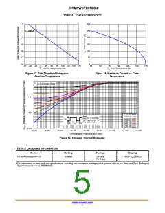
TYPICAL CHARACTERISTICS
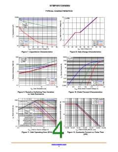
1.2
1.1
1
300
250
200
150
100
50
ID=330uA
0.9
0.8
0.7
0.6
0
−75 −50 −25
0
25
50
75 100 125 150 175
25
50
75
100
125
150
175
T
T
J, Junction Temperature (°C)
C, Case Temperature (°C)
Figure 13. Gate Threshold Voltage vs.
Junction Temperature
Figure 14. Maximum Current vs. Case
Temperature
1
D=0 is Single Pulse
0.1
0.01
D=0.00
D=0.01
D=0.02
D=0.05
D=0.10
D=0.20
D=0.50
Notes:
ZθθJJCC(t)=0.77°C/W Max
P
DM
TJM==PPDDMMxZθθJJCC((t)t)++TTC
Duty Cycle,D=t11//tt
t
1
2
t
2
0.001
1e−06
1e−05
1e−04
1e−03
1e−02
1e−01
1e+00
1e+01
1e+02
t, Rectangular Pulse Duration (sec)
Figure 15. Transient Thermal Response
DEVICE ORDERING INFORMATION
Device
†
Marking
Package
Shipping
NTMFWS1D5N08XT1G
1D5N08
DFNW5
(Pb−Free)
1500 / Tape & Reel
†For information on tape and reel specifications, including part orientation and tape sizes, please refer to our Tape and Reel Packaging
Specifications Brochure, BRD8011/D.
www.onsemi.com
5

 ONSEMI [ ONSEMI ]