NTMFWS1D5N08X
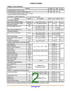
THERMAL CHARACTERISTICS
Parameter
Symbol
Value
0.77
39
Unit
Thermal Resistance, Junction−to−Case
R
°C/W
q
JC
Thermal Resistance, Junction−to−Ambient (Notes 4, 5)
R
q
JA
2
4. Surface−mounted on FR4 board using a 1 in , 1 oz. Cu pad.
5. R
is determined by the user’s board design.
q
JA
ELECTRICAL CHARACTERISTICS (T = 25°C unless otherwise specified)
J
Parameter
OFF CHARACTERISTICS
Symbol
Test Condition
Min
Typ
Max
Unit
Drain−to−Source Breakdown Voltage
V
V
GS
= 0 V, I = 1 mA
80
V
(BR)DSS
D
Drain−to−Source Breakdown Voltage
Temperature Coefficient
DV
/
I
D
= 1 mA, Referenced to 25°C
17.8
mV/°C
(BR)DSS
DT
J
Zero Gate Voltage Drain Current
I
V
= 80 V, T = 25°C
1
mA
nA
DSS
DS
J
V
DS
= 80 V, T = 125°C
250
100
J
Gate−to−Source Leakage Current
ON CHARACTERISTICS
I
V
= 0 V, V = 20 V
GSS
DS GS
Drain−to−Source On Resistance
R
V
= 10 V, I = 50 A
1.24
1.9
1.43
2.5
mW
DS(on)
GS
D
V
= 6 V, I = 33 A
D
GS
Gate Threshold Voltage
V
V
GS
V
GS
= V , I = 330 mA
2.4
3.6
V
GS(TH)
DS
D
Gate Threshold Voltage Temperature
Coefficient
DV
/
= V , I = 330 mA
−7.32
mV/°C
GS(TH)
DS
D
DT
J
Forward Transconductance
g
FS
V
DS
= 5 V, I = 50 A
176
S
D
CHARGES, CAPACITANCES & GATE RESISTANCE
Input Capacitance
Output Capacitance
Reverse Transfer Capacitance
Output Charge
C
5880
1690
25
pF
ISS
C
OSS
C
RSS
Q
OSS
V
= 0 V, V = 40 V, f = 1 MHz
DS
GS
121
51
nC
Total Gate Charge
Q
Q
V
= 6 V, V = 40 V; I = 50 A
GS DD D
G(TOT)
G(TOT)
Total Gate Charge
83
Threshold Gate Charge
Gate−to−Source Charge
Gate−to−Drain Charge
Gate Plateau Voltage
Gate Resistance
Q
18
G(TH)
Q
27
V
GS
= 10 V, V = 40 V; I = 50 A
DD D
GS
GD
GP
Q
V
13
4.6
0.6
V
R
f = 1 MHz
W
G
SWITCHING CHARACTERISTICS
Turn−On Delay Time
Rise Time
t
24
9
ns
d(ON)
Resistive Load,
t
r
V
= 0/10 V, V = 40 V,
GS
D
DD
Turn−Off Delay Time
Fall Time
t
43
9
d(OFF)
I
= 50 A, R = 2.5 W
G
t
f
SOURCE−TO−DRAIN DIODE CHARACTERISTICS
Forward Diode Voltage
V
V
= 0 V, I = 50 A, T = 25°C
0.81
0.66
32
1.2
V
SD
GS
S
J
V
GS
= 0 V, I = 50 A, T = 125°C
S J
Reverse Recovery Time
Charge Time
t
ns
RR
t
t
19
a
V
GS
= 0 V, I = 50 A,
S
dI/dt = 1000 A/ms, V = 40 V
Discharge Time
DD
13
b
Reverse Recovery Charge
Q
224
nC
RR
Product parametric performance is indicated in the Electrical Characteristics for the listed test conditions, unless otherwise noted. Product
performance may not be indicated by the Electrical Characteristics if operated under different conditions.
www.onsemi.com
2

 ONSEMI [ ONSEMI ]