NCV7703
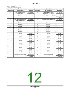
Table 4. Input Bit 15, Overvoltage Lock Out (OVLO) Shut Down
OVLO Input
Bit 15
V
OVLO
Output Data Bit 15 Power
Supply Fail (PSF) Status
S
Condition
OUTx Status
Unchanged
Unchanged
Unchanged
0
0
1
1
0
1
0
1
0
1 (Need SRR to reset)
0
1 (Need SRR to reset)
All Outputs Shut Off (Remain off until V is out of OVLO)
S
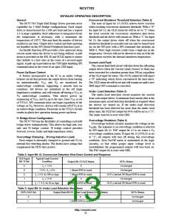
Thermal Shutdown
Three independent thermal shutdown circuits are featured
(one common sensor for each HS and LS transistor pair).
Each sensor has two temperature levels; Level 1, Thermal
Warning sets the “TW” status bit to a 1 and would have to
be reset with a command that includes the SRR after the IC
cools to a temperature below Level 1. The output will remain
on in this condition.
If the IC temperature reaches Level 2, Over Temperature
Shutdown, all drivers are latched off. It can be reset only
after the part cools below the shutdown temperature,
(including thermal hysteresis) with a turn−on command that
includes the SRR set bit.
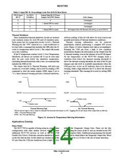
software polling of this bit will allow for load control and
possible prevention of thermal shutdown conditions.
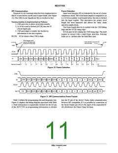
Thermal warning information can be retrieved
immediately without performing a complete SPI access
cycle. Figure 12 below displays how this is accomplished.
Bringing the CSB pin from a high to low condition
immediately displays the information on the Output Data Bit
0, thermal warning, even in the absence of an SCLK signal.
As the temperature of the NCV7703 changes from a
condition from below the thermal warning threshold to
above the thermal warning threshold, the state of the SO pin
changes and this level is available immediately when the
CSB goes low. A low on SO indicates there is no thermal
warning, while a high indicates the IC is above the thermal
warning threshold. This warning bit is reset by setting SRR
to “1”.
The output data bit 0, Thermal Warning, will latch and
remain set, even after cooling, and is reset by sending a SPI
command to reset the status register (SRR, input 0 set to
“1”). Since thermal warning precedes a thermal shutdown,
CSB
CSB
SCLK*
SCLK*
Tristate Level
SO
SO
TWH
NTW
Tristate Level
Thermal Warning High
No Thermal Warning
*SCLK can be high or low in order to maintain the thermal information on SO. Toggling SCLK will cause other output bits to shift out.
TWH = Thermal Warning High
NTW = No Thermal Warning
Figure 12. Access to Temperature Warning Information
Applications Drawing
Daisy Chain
The NCV7703 is capable of being setup in a daisy chain
configuration with other similar devices which include
additional NCV7703 devices as well as the NCV7708
Double Hex Driver. Particular attention should be focused
on the fact that the first 16 bits which are clocked out of the
SO pin when the CSB pin transitions from a high to a low
will be the Diagnostic Output Data. These are the bits
representing the status of the IC and are detailed in the SPI
Bit Description Table. Additional programming bits should
be clocked in which follow the Diagnostic Output bits. Word
length must be h x 16 due to the use of frame detection.
http://onsemi.com
14

 ONSEMI [ ONSEMI ]