NCV7703
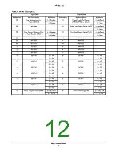
SPI Communication
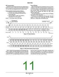
Frame Detection
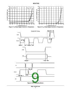
Standard 16−bit communication has been implemented to
this IC to turn drivers on/off, and to report faults. (See Figure
11). The LSB (Least Significant Bit) is clocked in first.
Input word integrity (SI) is evaluated by the use of a frame
consistency check. The word frame length is compared to an
h x 16 bit acceptable word length before the data is latched
into the input register. This guarantees the proper word
length has been imported and allows for daisy chain
operation applications.
The frame length detector is enabled with the CSB falling
edge and the SCLK rising edge.
SCLK must be low during the CSB rising edge. The fault
register is cleared with a valid frame detection. Existing
faults are re−latched after the fault filter time.
Communication is Implemented as Follows:
1. CSB goes low to allow serial data transfer.
2. A 16 bit word is clocked (SCLK) into the SI
(Serial Input) pin.
3. CSB goes high to transfer the clocked in
information to the data registers.
NOTE: SO is tristate when CSB is high.
Frame detection starts
after the CSB falling edge
and the SCLK rising edge.
Frame detection mode ends with
CSB rising edge.
CSB
SCLK
SI
SRR OUTL1 OUTH1 OUTL2 OUTH2 OUTL3 OUTH3
X
X
X
X
X
X
OCD
14
X
OVLO
16
Internal Counter
1
2
3
4
5
6
7
8
9
10
11
12
13
15
Valid 16 bits shown
Figure 10. Frame Detection
CSB
SRR OUTL1 OUTH1 OUTL2 OUTH2 OUTL3 OUTH3
X
X
X
X
X
X
X
X
X
OCD
X
OVLO
PSF
SI
SCLK
TW
OUTL1 OUTH1 OUTL2 OUTH2 OUTL3 OUTH3
X
X
X
OLD
ULD
SO
Figure 11. SPI Communication Frame Format
Table 1 defines the programming bits and diagnostic bits.
Figure 11 displays the timing diagram associated with Table
1. Fault information is sequentially clocked out the SO pin
of the NCV7703 as programming information is clocked
into the SI pin of the device. Daisy chain communication
between SPI compatible IC’s is possible by connection of
the Serial Output pin (SO) to the input of the sequential IC
(SI) (Reference the Daisy Chain Section).
http://onsemi.com
11

 ONSEMI [ ONSEMI ]