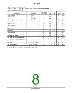
NCV7703
DETAILED OPERATING DESCRIPTION
General
Overcurrent Shutdown Threshold Detection (Table 2)
The NCV7703 Triple Half Bridge Driver provides drive
The state of input bit 13 (OCD) selects driver reaction
when reaching overcurrent shutdown threshold. With a “0”
for input bit 13, the OLD status bit will be set to “1” when
the level exceeds the overcurrent shutdown shut−down
threshold and the driver will remain on. With a “1” for input
bit 13, the output driver shuts off when the overcurrent
shutdown threshold is exceeded and can only be turned back
on via the SPI port with a SPI command that includes an
SRR=1. Note: high currents could cause a high rise in die
temperature. Devices will not be allowed to turn on if the die
temperature exceeds the thermal shutdown temperature.
capability for 3 Half−Bridge configurations. Each output
drive is characterized for a 500 mA load and has a typical
1.4 A surge capability. Strict adherence to integrated circuit
die temperature is necessary, with a maximum die
temperature of 150°C. This may limit the number of drivers
enabled at one time. Output drive control and fault reporting
are handled via the SPI (Serial Peripheral Interface) port.
An Enable function (EN) provides a low quiescent sleep
current mode when the device is not being utilized. A pull
down is provided on the EN, SI and SCLK inputs to ensure
they default to a low state in the event of a severed input
signal. A pull−up is provided on the CSB input disabling SPI
communication in the event of an open CSB input.
Current Limit Fault
The current limit fault circuit will shut down the offending
output driver when the Current Limit (Source or Sink) has
been exceeded for a duration greater than 200 ms, regardless
of the OLD input bit status. The OUTx output bit will report
a “0” indicating which driver encountered the hard short.
The OLD status bit will be set and will remain set until a new
SRR input SPI command is executed.
Power Up/Down Control
A feature incorporated in the IC is an under voltage
lockout circuit that prevents the output drivers from turning
on unintentionally. V
and V are monitored for
CC
S
undervoltage conditions supporting a smooth turn−on
transition. All drivers are initialized in the off (high
Under−Load Detection (Table 3)
impedance) condition, and will remain off during a V or
CC
The under−load detection circuit monitors the current
from each output driver. A minimum load current (this is the
maximum open circuit detection threshold) is required when
the drivers are turned on. If the under−load detection
threshold has been detected for more than the under−load
delay time, the ULD bit (output bit #14) will be set to a “1”.
The under load bit is reset with SRR.
V
undervoltage condition. This allows power up
S
sequencing of V , and V up to the user. Once V is out
of UVLO, SPI communication can begin regardless of the
voltage on V . However, drivers will remain off if V is in
an undervoltage condition. Hysteresis in the UVLO circuits
results in glitch free operation during power up/down.
CC
S
CC
S
S
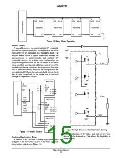
H−Bridge Driver Configuration
Overvoltage Shutdown (Table 4)
Overvoltage lockout circuitry monitors the voltage on the
The NCV7703 has the flexibility of controlling each half
bridge driver independently. This allows for high side, low
side and H−bridge control. H−bridge control provides
forward, reverse, brake and high impedance states.
V pin. The response to an overvoltage condition is selected
S
by SPI input bit 15. PSF output bit 15 is set when a V
S
overvoltage condition exists. If input bit 15 (OVLO) is set
to “1”, all outputs will turn off during this overvoltage
condition. Turn On/Off status is maintained in the logic
circuitry, so that when proper input voltage level is
reestablished, the programmed outputs will turn back on.
The PSF output bit is reset with SRR.
Overvoltage Clamping − Driving Inductive Loads
Each output is internally clamped to ground and Vs by
internal free wheeling diodes. The diodes have ratings that
complement the FETs they protect.
Table 2. Input Bit 13, Overcurrent Detection Shut Down Control and Response
OLD Input
Bit 13 Set
Typical Load Current
Condition
Output Bit 13 OLD Status
OUTx Status
Unchanged
0
0
0
1
1
I
L
≤ 1.4 A
0
1.4 A < I ≤ 3 A
1 (Need SRR to reset)
1 (Need SRR to reset)
0
Unchanged
L
I
≥ 3 A, for 200 ms (typ)
OUTx Latched Off (Need SRR to reset)
Unchanged
L
I
L
≤ 1.4 A
I > 1.4 A, for 25 ms (typ)
L
1 (Need SRR to reset)
OUTx Latched Off (Need SRR to reset)
Table 3. Input Bit 14, Under Load Detection Shut Down
OUTx ULD Set
Output Data Bit 14, Under Load Detect (ULD) Status
OUTx Status
Unchanged
Unchanged
0
1
0
1 (Need SRR to reset)
http://onsemi.com
13

 ONSEMI [ ONSEMI ]