NCS37020
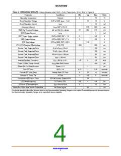
The ground fault detection circuit has different levels of
time delay before the SCR is enabled:
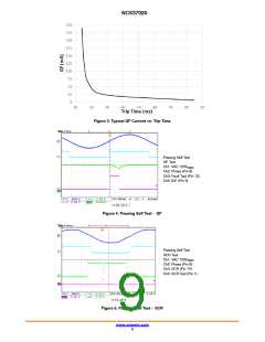
Figure 5 shows a passing self−test SCR test. This test
checks for the SCR and bias circuitry. Channel 1 shows the
VAC 120 V
, 60 Hz Line Voltage. Channel 2 shows the
RMS
6 mA to 15 mA
15 mA to 30 mA
30 mA to 100 mA
>100 mA
If a very high GF occurs and a greater than 250 mV signal
occurs across the CT for greater than 1.4 ms, the saturation
fault comparator will enable the SCR during the positive
half cycle.
During a self−test, the GF detection circuit is active.
However, for the 6 mA to 15 mA GF range, an additional
~100ms trip delay will be added before the SCR is enabled.
Note that the above equation is for an ideal CT. In practice,
the GF threshold can be 30% different and should be
empirically set.
The internal oscillator is trimmed to 2 MHz when the AC
frequency is 60 Hz. If the AC frequency is lower, the GF trip
threshold response time will be slower.
≤150 ms
≤100 ms
≤40 ms
≤25 ms
positive and negative phase half wave cycles. Channel 3
shows the SCR signal and channel 4 shows the SCR Test
signal. At the end of the positive half cycle, the SCR Test pin
is biased high. Approximately 3 ms into the negative half
wave cycle, the SCR is enabled high. This causes the SCR
Test pin to go low. When it goes below ~2.1 volts, a passing
SCR test is recorded and the SCR signal is disabled.
After a passing self−test cycle per Figures 4 and5, the next
ST cycle will occur in 720 seconds.
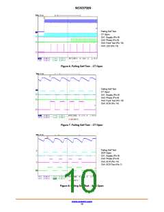
Figure 6 shows a failing ST cycle for an open CT. Channel
1 shows the NCS37020 supply voltage. Channel 2 shows the
phase pin. Channel 3 shows the Fault Test signal and channel
4 shows the LED (End of Life) signal. The first four
consecutive ST cycles occur at about 1.1 seconds, then at
th
2.2, 3.3 and 4.4 seconds. After the 16 consecutive cycle
failure, the SCR is enabled for four positive half cycles and
then the LED is enabled.
The CT sense amplifier has an internal dynamic V
cancelation circuit which allows for direct coupling to the
CT transformer.
The TE pin is used for internal production testing only.
This pin should be connected to the GND pin.
Contact onsemi for self−test requirement details and
noise filtering recommendations.
Figure 7 also shows a failing ST cycle for an open CT. It
is a zoom figure for the first four consecutive ST cycles. It
shows the same waveforms as Figure 6 but channel 4 shows
the SCR pin. Comparing Figure 7 with Figure 4, it can be
observed that the Fault Test pin is enabled for the complete
positive half wave cycle because no GF signal is detected by
the NCS37020.
OS
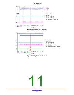
Figure 8 shows a failing ST cycle for an open SCR.
Channel 1 shows the supply voltage, channel 2 shows the
Phase pin, channel 3 shows the SCR pin and channel 4 shows
the SCR Test pin. The SCR is enabled inside the negative
half wave cycle. The SCR Test pin does not detect the SCR
going low so the cycle is recorded as a SCR failure test.
Figure 9 shows a failing “no clock” test. The Phase pin is
floating for this test. Channel 1 shows the supply voltage,
channel 2 shows the Phase pin and channel 3 shows the LED
pin. No signal is present on the Phase pin after POR. At
~114 ms, the LED End of Life signal is enabled during the
positive half wave cycle. The LED EOL signal blinks at
4 Hz.
Figure Description
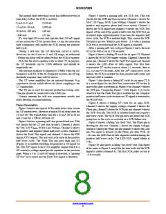
Figure 3 shows the typical SCR enable delay time versus
the GF current level. Shown is a typical 85 ms delay time for
a 6 mA GF. The typical delay time for a 25 mA GF is 28 ms
and 14 ms for a 500 W 240 mA GF.
Figure 4 shows a passing self−test ground fault test. This
test checks for the CT and bias circuitry. Channel 1 shows
the VAC 120 V , 60 Hz Line Voltage. Channel 2 shows
RMS
the positive and negative phase half wave cycles. Channel 3
shows the Fault Test signal and channel 4 shows the IDF
signal (CTO output). The self−test cycle starts in the positive
half wave cycle. The Fault Test pin goes high and Q2
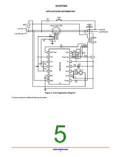
(Figure 2) is enabled. Enabling Q2 generates a GF signal via
R8. The IDF signal is the CTO amplifier output which is a
GF current to voltage signal per the equation on the previous
page. When a 5 to 15 mA GF signal is detected, a “passing
GF test” is recorded and the Fault Test signal is disabled.
Figure 10 also shows a failing “no clock” test. This figure
is the same as Figure 9 except for the time scale and the SCR
signal is added (channel 4). The first SCR pulse occurs at
~3.8 seconds.
www.onsemi.com
8

 ONSEMI [ ONSEMI ]