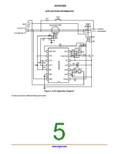
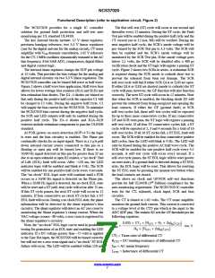
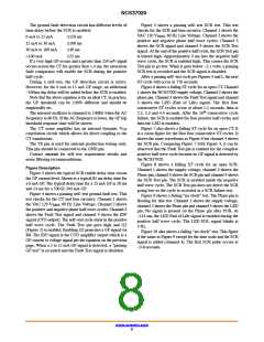
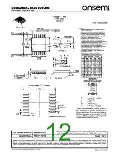
MECHANICAL CASE OUTLINE
PACKAGE DIMENSIONS
TSSOP−14 WB
CASE 948G
ISSUE C
14
DATE 17 FEB 2016
1
SCALE 2:1
NOTES:
14X K REF
1. DIMENSIONING AND TOLERANCING PER
ANSI Y14.5M, 1982.
M
S
S
V
0.10 (0.004)
T U
2. CONTROLLING DIMENSION: MILLIMETER.
3. DIMENSION A DOES NOT INCLUDE MOLD
FLASH, PROTRUSIONS OR GATE BURRS.
MOLD FLASH OR GATE BURRS SHALL NOT
EXCEED 0.15 (0.006) PER SIDE.
4. DIMENSION B DOES NOT INCLUDE
INTERLEAD FLASH OR PROTRUSION.
INTERLEAD FLASH OR PROTRUSION SHALL
NOT EXCEED 0.25 (0.010) PER SIDE.
5. DIMENSION K DOES NOT INCLUDE DAMBAR
PROTRUSION. ALLOWABLE DAMBAR
PROTRUSION SHALL BE 0.08 (0.003) TOTAL
IN EXCESS OF THE K DIMENSION AT
MAXIMUM MATERIAL CONDITION.
S
0.15 (0.006) T U
N
0.25 (0.010)
14
8
2X L/2
M
B
L
N
−U−
PIN 1
IDENT.
F
7
1
6. TERMINAL NUMBERS ARE SHOWN FOR
REFERENCE ONLY.
DETAIL E
7. DIMENSION A AND B ARE TO BE
DETERMINED AT DATUM PLANE −W−.
S
K
0.15 (0.006) T U
A
−V−
MILLIMETERS
DIM MIN MAX
INCHES
MIN MAX
K1
A
B
C
D
F
G
H
J
4.90
4.30
−−−
0.05
0.50
5.10 0.193 0.200
4.50 0.169 0.177
J J1
1.20
−−− 0.047
0.15 0.002 0.006
0.75 0.020 0.030
SECTION N−N
0.65 BSC
0.026 BSC
0.60 0.020 0.024
0.20 0.004 0.008
0.16 0.004 0.006
0.30 0.007 0.012
0.25 0.007 0.010
0.50
0.09
0.09
0.19
J1
K
−W−
C
K1 0.19
L
M
6.40 BSC
0.252 BSC
0.10 (0.004)
0
8
0
8
_
_
_
_
SEATING
PLANE
−T−
H
G
DETAIL E
D
GENERIC
MARKING DIAGRAM*
14
SOLDERING FOOTPRINT
XXXX
XXXX
ALYWG
G
7.06
1
1
A
L
= Assembly Location
= Wafer Lot
Y
W
G
= Year
= Work Week
= Pb−Free Package
0.65
PITCH
(Note: Microdot may be in either location)
*This information is generic. Please refer to
device data sheet for actual part marking.
Pb−Free indicator, “G” or microdot “G”, may
or may not be present. Some products may
not follow the Generic Marking.
01.34X6
14X
1.26
DIMENSIONS: MILLIMETERS
Electronic versions are uncontrolled except when accessed directly from the Document Repository.
Printed versions are uncontrolled except when stamped “CONTROLLED COPY” in red.
DOCUMENT NUMBER:
DESCRIPTION:
98ASH70246A
TSSOP−14 WB
PAGE 1 OF 1
onsemi and
are trademarks of Semiconductor Components Industries, LLC dba onsemi or its subsidiaries in the United States and/or other countries. onsemi reserves
the right to make changes without further notice to any products herein. onsemi makes no warranty, representation or guarantee regarding the suitability of its products for any particular
purpose, nor does onsemi assume any liability arising out of the application or use of any product or circuit, and specifically disclaims any and all liability, including without limitation
special, consequential or incidental damages. onsemi does not convey any license under its patent rights nor the rights of others.
© Semiconductor Components Industries, LLC, 2019
www.onsemi.com

 ONSEMI [ ONSEMI ]