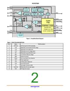
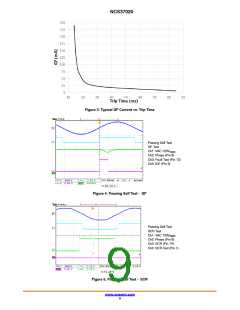
NCS37020
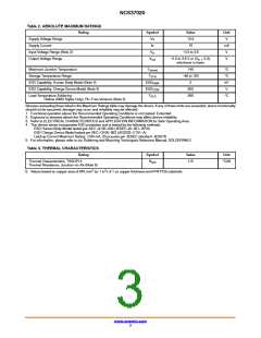
Table 2. ABSOLUTE MAXIMUM RATINGS
Rating
Symbol
Value
13.5
Unit
V
Supply Voltage Range
Supply Current
Vs
Is
10
mA
V
Input Voltage Range (Note 3)
Output Voltage Range
V
in
−0.3 to 3.6
V
out
−0.3 to 3.6 V or (V + 0.3),
V
in
whichever is lower
Maximum Junction Temperature
T
140
−65 to 150
2
°C
°C
kV
V
J(max)
Storage Temperature Range
T
STG
ESD Capability, Human Body Model (Note 4)
ESD Capability, Charge Device Model (Note 4)
Lead Temperature Soldering
ESD
ESD
HBM
CDM
500
T
260
°C
SLD
Reflow (SMD Styles Only), Pb−Free Versions (Note 5)
Stresses exceeding those listed in the Maximum Ratings table may damage the device. If any of these limits are exceeded, device functionality
should not be assumed, damage may occur and reliability may be affected.
1. Functional operation above the Recommended Operating Conditions is not implied. Extended
2. Exposure to stresses above the Recommended Operating Conditions may affect device reliability.
3. Refer to ELECTRICAL CHARACTERISTICS and APPLICATION INFORMATION for Safe Operating Area.
4. This device series incorporates ESD protection and is tested by the following methods:
ESD Human Body Model tested per AEC−Q100−002 (JEDEC JS−001−2010)
ESD Charge Device Model tested per AEC−Q100−003 (JESD22−C101−A)
Latchup Current Maximum Rating: ≤100 mA, 20 ms pulse per JEDEC standard: JESD78
5. For information, please refer to our Soldering and Mounting Techniques Reference Manual, SOLDERRM.D
Table 3. THERMAL CHARACTERISTICS
Rating
Symbol
Value
Unit
Thermal Characteristics, TSSOP14
Thermal Resistance, Junction−to−Air (Note 6)
R
115
°C/W
θJA
2
2
6. Values based on copper area of 645 mm (or 1 in ) of 1 oz copper thickness and FR4 PCB substrate.
www.onsemi.com
3

 ONSEMI [ ONSEMI ]