NCP3170
VIN
VDD
EN
Power
Control
(PC)
UVLO
POR
Driver
Voltage
Clamp
VCV
VCL
Soft Start
Reference
Slope
Compensation
0.030 V/A
Current
Sense
S
ORing
Circuit
Pulse by
Pulse
Current
Limit
SET
Oscillator
S
Q
Q
+
FB
R
CLR
+
−
−
VIN
COMP
Soft Start
Complete
Logic
HS
PDRV
+
VSW
VCW
VCL
−
998 mV
+
hs
867 mV
728 mV
−
+
−
LS
NDRV
PG
VSW
Over
Zero
Temperature
Protection
Current
Detection
AGND
PGND
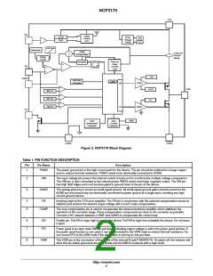
Figure 2. NCP3170 Block Diagram
Description
Table 1. PIN FUNCTION DESCRIPTION
Pin
Pin Name
1
PGND
The power ground pin is the high current path for the device. The pin should be soldered to a large copper
area to reduce thermal resistance. PGND needs to be electrically connected to AGND.
2
3
VIN
The input voltage pin powers the internal control circuitry and is monitored by multiple voltage comparators.
The VIN pin is also connected to the internal power PMOS switch and linear regulator output. The VIN pin
has high di/dt edges and must be decoupled to ground close to the pin of the device.
AGND
The analog ground pin serves as small-signal ground. All small-signal ground paths should connect to the
AGND pin and should also be electrically connected to power ground at a single point, avoiding any high
current ground returns.
4
5
FB
Inverting input to the OTA error amplifier. The FB pin in conjunction with the external compensation serves to
stabilize and achieve the desired output voltage with current mode compensation.
COMP
The loop compensation pin is used to compensate the transconductance amplifier which stabilizes the
operation of the converter stage. Place compensation components as close to the converter as possible.
Connect a RC network between COMP and AGND to compensate the control loop.
6
7
EN
PG
Enable pin. Pull EN to logic high to enable the device. Pull EN to logic low to disable the device. Do not leave
it open.
Power good is an open drain 500 mA pull down indicating output voltage is within the power good window. If
the power good function is not used, it can be connected to the VSW node to reduce thermal resistance. Do
not connect PG to the VSW node if the application is turning on into pre-bias.
8
VSW
The VSW pin is the connection of the drains of the internal N and P MOSFETS. At switch off, the inductor will
drive this pin below ground as the body diode and the NMOS conducts with a high dv/dt.
http://onsemi.com
2

 ONSEMI [ ONSEMI ]