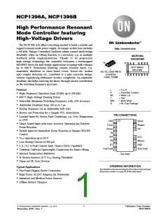
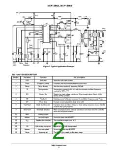
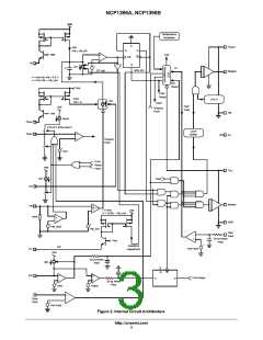
NCP1396A, NCP1396B
ELECTRICAL CHARACTERISTICS
(For typical values T = 25C, for min/max values T = --40C to +125C, Max T = 150C, V = 12 V, unless otherwise noted.)
J
J
J
CC
Characteristic
Pin
Symbol
Min
Typ
Max
Unit
SUPPLY SECTION
Turn--on threshold level, V going up – A version
12
12
VCC
VCC
12.3
9.5
8.5
8
13.4
10.5
9.5
9
14.3
11.5
10.5
10
V
V
CC
ON
ON
Turn--on threshold level, V going up – B version
CC
Minimum operating voltage after turn--on
Startup voltage on the floating section
Cutoff voltage on the floating section
12
VCC
V
(min)
16--14
16--14
12
Vboot
V
ON
Vboot
7.4
8.4
9.4
V
(min)
Startup current, V < VCC
0C < T < +125C
Istartup
--
--
--
--
300
350
mA
CC
ON
J
-- 4 0 C < T < +125C
J
V
level at which the internal logic gets reset
12
12
VCC
--
--
6.5
4
--
--
V
CC
reset
Internal IC consumption, no output load on pin 15/14 – 11/10, Fsw =
300 kHz
ICC1
mA
Internal IC consumption, 1 nF output load on pin 15/14 – 11/10, Fsw =
300 kHz
12
12
ICC2
ICC3
--
--
11
--
--
mA
mA
Consumption in fault mode (All drivers disabled, V > V
CC
)
1.2
CC(min)
VOLTAGE CONTROL OSCILLATOR (VCO)
Characteristic
Pin
Symbol
Min
Typ
Max
Unit
Minimum switching frequency, Rt = 18 kΩ on pin 4, Vpin 6 = 0.8 V, DT =
300 ns
4
Fsw min
58.2
60
61.8
kHz
Maximum switching frequency, Rfmax = 1.3 kΩ on pin 2, Vpin 6 > 5.3 V,
Rt = 18 kΩ, DT = 300 ns
2
Fsw max
425
500
575
kHz
Feedback pin swing above which Δf = 0
Operating duty--cycle symmetry
6
11--15
--
FBSW
DC
--
48
--
5.3
50
20
--
52
--
V
%
ms
Delay before any driver re--start in fault mode
Tdel
FEEDBACK SECTION
Characteristic
Pin
6
Symbol
Rfb
Min
Typ
20
Max
Unit
kΩ
V
Internal pull--down resistor
--
--
--
--
--
--
Voltage on pin 6 below which the FB level has no VCO action
Voltage on pin 6 below which the controller considers a fault
6
Vfb_min
Vfb_off
1.2
0.6
6
V
DRIVE OUTPUT
Characteristic
Pin
Symbol
Min
Typ
Max
Unit
Output voltage rise--time @ CL = 1 nF, 10--90% of output signal
Output voltage fall--time @ CL = 1 nF, 10--90% of output signal
Source resistance
15--14/1
1--10
T
--
40
--
ns
r
15--14/1
1--10
T
f
--
--
--
20
13
--
--
--
ns
Ω
15--14/1
1--10
R
OH
Sink resistance
15--14/1
1--10
R
5.5
Ω
OL
Dead time with R = 10 kΩ from pin 7 to GND
7
7
7
T_dead
250
300
2
340
--
ns
ms
ns
mA
DT
Maximum dead--time with R = 82 kΩ from pin 7 to GND
T_dead--max
T_dead--min
IHV_LEAK
--
--
--
DT
Minimum dead--time, R = 3 kΩ from pin 7 to GND
100
--
--
DT
Leakage current on high voltage pins to GND
14,
15,16
5
http://onsemi.com
5

 ONSEMI [ ONSEMI ]